Pinout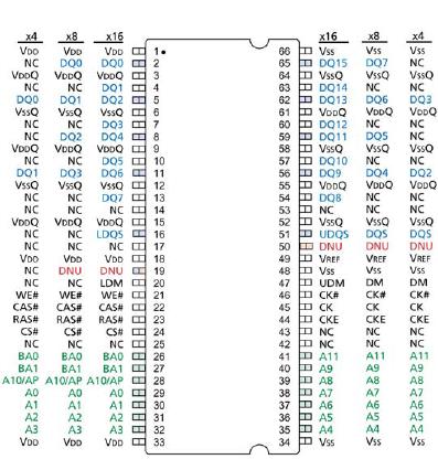 SpecificationsVDD Supply Voltage
Relative to VSS .............................................................................-1V to +3.6V
VDDQ Supply
Voltage Relative to VSS ................................................................ -1V to +3.6V
VREF and Inputs Voltage
Relative to VSS ...............................................................................-1V to +3.6V
I/O Pins Voltage
Relative to VSS ..................................................................-0.5V to VDDQ +0.5V
Operating Temperature, TA (ambient) .................................... 25°C to +70°C
Storage Temperature (plastic) ............................................. -55°C to +150°C
Power Dissipation ..........................................................................................1W
Short Circuit Output Current .......................................................................50mADescriptionThe 128Mb: x4, x8, x16 SDRAM is a high-speed CMOS, dynamic random-access memory containing 134,217,728 bits. It is internally configured as a quad-bank DRAM.
The 128Mb: x4, x8, x16 SDRAM uses a double data rate architecture to achieve high-speed operation. The double data rate architecture is essentially a 2n-prefetch architecture with an interface designed to transfer two data words per clock
cycle at the I/O pins. A single read or write access for the 128Mb DDR SDRAM effectively consists of a single 2n-bit wide, one-clock-cycle data transfer at the internal DRAM core and two corresponding n-bit wide, one-half-clock-cycle data transfers at the I/O pins.
A bi-directional data strobe (DQS) is transmitted externally, along with data, for use in data capture at the receiver. DQS is a strobe transmitted by the DDR SDRAM during READs and by the memory controller during WRITEs. DQS is edge-aligned with data for READs and center-aligned with data for WRITEs. The x16 offering has two data strobes,
one for the lower byte and one for the upper byte.
The 128Mb: x4, x8, x16 SDRAM operates from a differential clock (CK and CK#); the crossing of CK going HIGH and CK# going LOW will be referred to as the positive edge of CK. Commands (address and control signals) are registered at every positive edge of CK. Input data is registered on both edges of DQS, and output data is referenced to both edges of
DQS, as well as to both edges of CK.
Read and write accesses to the DDR SDRAM are burst oriented; accesses start at a selected location and continue for
a programmed number of locations in a programmed sequence. Accesses begin with the registration of an ACTIVE
command, which is then followed by a READ or WRITE command. The address bits registered coincident with the
ACTIVE command are used to select the bank and row to be accessed. The address bits registered coincident with the READ or WRITE command are used to select the bank and the starting column location for the burst access.
The 128Mb: x4, x8, x16 SDRAM provides for programmable READ or WRITE burst lengths of 2, 4, or 8 locations. An auto precharge function may be enabled to provide a self-timed row precharge that is initiated at the end of the burst access.
As with standard SDR SDRAMs, the pipelined, multibank architecture of DDR SDRAMs allows for concurrent operation, thereby providing high effective bandwidth by hiding row precharge and activation time.
An auto refresh mode is provided, along with a powersaving power-down mode. All inputs are compatible with the
JEDEC Standard for SSTL_2. All full drive strength outputs are SSTL_2, Class II compatible.

 128Mb: x4, x8, x16 Data Sheet


