Features: • VDD = +2.5V ±0.2V, VDDQ = +2.5V ±0.2V
• Bidirectional data strobe (DQS) transmitted/ received with data, i.e.,
source-synchronous data capture (x16 has two one per byte)
• Internal, pipelined double-data-rate (DDR) architecture; two data accesses
per clock cycle
• Differential clock inputs (CK and CK#)
• Commands entered on each positive CK edge
• DQS edge-aligned with data for READs; center- aligned with data for WRITEs
• DLL to align DQ and DQS transitions with CK
• Four internal banks for concurrent operation
• Data mask (DM) for masking write data (x16 has two one per byte)
• x16 has programmable IOL/IOH option
• Programmable burst lengths: 2, 4, or 8
• Auto precharge option
• Auto Refresh and Self Refresh Modes
• Longer lead TSOP for improved reliability (OCPL)
• 2.5V I/O (SSTL_2 compatible)Pinout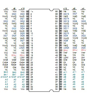 Specifications
VDD Supply Voltage
Relative to VSS ...................................... -1V to +3.6V
VDDQ Supply
Voltage Relative to VSS ......................... -1V to +3.6V
VREF and Inputs Voltage
Relative to VSS ...................................... -1V to +3.6V
I/O Pins Voltage
Relative to VSS .......................... -0.5V to VDDQ +0.5V
Operating Temperature, TA (ambient) ........ 0 to +70
Storage Temperature (plastic) .............. -55 to +150
Power Dissipation .................................................... 1W
Short Circuit Output Current ................................ 50mA
*Stresses greater than those listed under "Absolute Maximum Ratings" may cause permanent damage to the device. This is a stress rating only, and functional operation of the device at these or any other condi- tions above those indicated in the operational sections of this specification is not implied. Exposure to abso- lute maximum rating conditions for extended periods may affect reliability.
DescriptionThe 128Mb DDR SDRAM is a high-speed CMOS, dynamic random-access memory containing 134,217,728 bits. It is internally configured as a quad- bank DRAM.
The 128Mb DDR SDRAM uses a double data rate architecture to achieve high-speed operation. The double data rate architecture is essentially a 2n-prefetch architecture with an interface designed to transfer two data words per clock cycle at the I/O pins. A single read or write access for the 128Mb DDR SDRAM effectively
consists of a single 2n-bit wide, one-clock-cycle data transfer at the internal DRAM core and two corre- sponding n-bit wide, one-half-clock-cycle data trans- fers at the I/O pins.
A bidirectional data strobe (DQS) is transmitted externally, along with data, for use in data capture at the receiver. DQS is a strobe transmitted by the DDR SDRAM during READs and by the memory controller during WRITEs. DQS is edge-aligned with data for READs and center-aligned with data for WRITEs. The x16 offering has two data strobes, one for the lower byte and one for the upper byte.
The 128Mb DDR SDRAM operates from a differen- tial clock (CK and CK#); the crossing of CK going HIGH and CK# going LOW will be referred to as the positive edge of CK. Commands (address and control signals) are registered at every positive edge of CK. Input data is registered on both edges of DQS, and output data is referenced to both edges of DQS, as well as to both edges of CK.
Read and write accesses to the 128Mb DDR SDRAM are burst oriented; accesses start at a selected location and continue for a programmed number of locations in a programmed sequence. Accesses begin with the regis- tration of an ACTIVE command, which is then fol- lowed by a READ or WRITE command. The address bits registered coincident with the ACTIVE command are used to select the bank and row to be accessed. The address bits registered coincident with the READ or
WRITE command are used to select the bank and the starting column location for the burst access.
The 128Mb DDR SDRAM provides for programmable READ or WRITE burst lengths of 2, 4, or 8 locations. An auto precharge function may be enabled to provide a self- timed row precharge that is initiated at the end of the burst access.
As with standard SDR SDRAMs, the pipelined, multibank architecture of DDR SDRAMs allows for concurrent operation, thereby providing high effective bandwidth by hiding row precharge and activation time.
An auto refresh mode is provided, along with a power-saving power-down mode. All inputs are com- patible with the JEDEC Standard for SSTL_2. All full drive strength outputs are SSTL_2, Class II compatible.
NOTE 1: The functionality and the timing specifications discussed in this
data sheet are for the DLL-enabled mode of operation.
NOTE 2: Throughout the data sheet, the various figures and text refer to DQs
as "DQ." The DQ term is to be interpreted as any and all
DQ collectively, unless specifically stated otherwise. Additionally,
the x16 is divided in to two bytes - the lower byte and upper byte.
For the lower byte (DQ0 through DQ7) DM refers to LDM and DQS
refers to LDQS; and for the upper byte (DQ8 through DQ15) DM refers
to UDM and DQS refers to UDQS.

 128Mb Data Sheet


