Features: · Designed to Operate Over Wide Supply Voltages of 5.5 to 26.5 V
· Interfaces to Microprocessor Using 8-Bit SPI I/O Protocol up to 3.0 MHz
· 1.0 A Peak Current Outputs with Maximum RDS(on) of 1.6 Ω at TJ - 150°C
· Outputs Current Limited to Accommodate In-rush Currents Associated with Switching Incandescent Loads
· Output Voltages Clamped to 53 V During Inductive Switching
· Maximum Sleep Current (IPWR) of 25 µA
· Maximum of 4.0 mA IDD During OperationPinout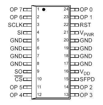 Specifications
| Rating |
Symbol |
Value |
Unit |
Power Supply Voltage
Normal Operation (Steady-State)
Transient Conditions (Note 1) |
V PWR(SS)
VPWR(PK) |
- 1.5 to 26.5
- 13 to 60 |
V
V
V |
Logic Supply Voltage (Note 2)
Input Pin Voltage (Note 3)
Output Clamp Voltage (Note 4)
2.0 mA IOUT 0.5 A |
VDD
VIN
VOUT(OFF) |
- 0.3 to 7.0
- 0.3 to 7.0
50 to 75 |
V
A
A |
Output Self-Limit Current
Continuous Per Output Current (Note 5)
ESD Voltage (Note 6)
Human Body Model (Note 7)
Machine Model (Note 8) |
IOUT(LIM)
IOUT(CONT)
VESD1
VESD2 |
3.0 to 6.0
1.0
2000
200 |
V |
Output Clamp Energy (Note 9)
Repetitive:
TJ = 25°C
TJ = 124°C
Non-Repetitive:
TJ = 25°C
TJ = 124°C |
ECLAMP |
100
30
2.0
0.5
|
mJ
mJ
J
J
|
Recommended Frequency of SPI Operation (Note 11)
Storage Temperature
Operating Case Temperature
Operating Junction Temperature
Power Dissipation (TA = 25°C) (Note 12)
Soldering Temperature (Note 13) |
fSPI
TSTG
TC
TJ
PD
TSOLDER |
2.0
- 55 to 150
- 40 to 125
- 40 to 150
3.0
260 |
MHz
°C
°C
°C
W
°C |
Notes:
1. Transient capability with external 100 Ω resistor in series with VP pin and supply.
2. Exceeding these limits may cause a malfunction or permanent damage to the device.
3. Exceeding the limits on SCLK, SI, CS, SFPD, or RST pins may cause permanent damage to the device.
4. With output OFF.
5. Continuous output current rating so long as maximum junction temperature is not exceeded. Operation at 125°C ambient temperature will require maximum output current computation using package RJA.
6. ESD data available upon request.
7. ESD1 testing is performed in accordance with the Human Body Model (CZap = 200 pF, RZap = 1500 Ω).
8. ESD2 testing is performed in accordance with the Machine Model (CZap = 200pF, RZap = 0 Ω).
9. Maximum output clamp energy capability at 150°C junction temperature using a single non-repetitive pulse method.
10. Guaranteed and production tested for 2.0 MHz SPI operation, but demonstrated to operate to 8.5 MHz at 25°C.
11. See Figure 20 for Thermal model.
12. Soldering temperature limit is for 10 seconds maximum duration; not designed for immersion soldering; exceeding these limits may cause malfunction or permanent damage to the device.Contact Motorola Sales Office for device immersion soldering time/temperature limits.
DescriptionThe 33298 device is an eight output, low side power switch with 8-bit serial input control. The 33298 is a versatile circuit designed for automotive applications, but is well suited for other environments. The 33298 incorporates SMARTMOS technology, with CMOS logic, bipolar/MOS analog circuitry, and DMOS power MOSFETs. The 33298 interfaces directly with a microcontroller to control various inductive or incandescent loads.
The circuits innovative monitoring and protection features include: Very Low Standby Current, SPI Cascade Fault Reporting Capability, Internal 53 V Clamp on Each Output, Output Specific Diagnostics, Independent Shutdown of Outputs.
The device is parametrically specified over an ambient temperature range of -40°C TA 125°C and 9.0 V VPWR 16 V supply.

 33298 Data Sheet


