33689D

Features: •Full-Duplex SPI Interface at Frequencies up to 4.0 MHz•LIN Transceiver Capable to 100 kbps with Waveshaping Capability•5.0 V Low Dropout Regulator Full Fault Detection and Protection•One 50 mA and Two 150 mA Protected High-Side Switches•Current Sense Operat...

product image

33689D Picture
SeekIC No. : 004228512 Detail

33689D: Features: •Full-Duplex SPI Interface at Frequencies up to 4.0 MHz•LIN Transceiver Capable to 100 kbps with Waveshaping Capability•5.0 V Low Dropout Regulator Full Fault Detection a...

floor Price/Ceiling Price

Part Number:
33689D
Supply Ability:
5000

Price Break

  • Qty
  • 1~5000
  • Unit Price
  • Negotiable
  • Processing time
  • 15 Days
Total Cost: $ 0.00

SeekIC Buyer Protection PLUS - newly updated for 2013!

  • Escrow Protection.
  • Guaranteed refunds.
  • Secure payments.
  • Learn more >>

Month Sales

268 Transactions

Rating

evaluate  (4.8 stars)

Upload time: 2024/4/26

Payment Methods

All payment methods are secure and covered by SeekIC Buyer Protection PLUS.

Notice: When you place an order, your payment is made to SeekIC and not to your seller. SeekIC only pays the seller after confirming you have received your order. We will also never share your payment details with your seller.
Product Details

Description


Features:

•Full-Duplex SPI Interface at Frequencies up to 4.0 MHz
•LIN Transceiver Capable to 100 kbps with Waveshaping Capability
•5.0 V Low Dropout Regulator Full Fault Detection and Protection
•One 50 mA and Two 150 mA Protected High-Side Switches
•Current Sense Operational Amplifier
•The 33689 is compatible with LIN 2.0 Specification Package.
•Pb-Free Packaging Designated by Suffix Code EW


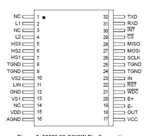
Pinout

  Connection Diagram


Specifications

Ratings Symbol Value Unit
ELECTRICAL RATINGS
VPWR Supply Voltage at VS1 and VS2
Continuous
Transient (Load Dump)
VSUPDC
VSUPTR
- 0.3 to 27
40
V
Supply Voltage at VDD and VCC VDD -0.3 to 5.5 V
Output Current at VDD IDD Internally Limited A
Logic Input Voltage at MOSI, SCLK, CS, IN, and TXD VINLOG -0.3 to VDD+0.3 V
Logic Output Voltage at MISO, INT, RST, and RXD VOUTLOG -0.3 to VDD+0.3 V
Input Voltage at E+ and E- VE+/VE- -0.3 to 7.0 V
Input Current at E+ and E- IE+/IE- ±20 mA
Output Voltage at OUT VOUT -0.3 to VCC+0.33 V
Output Current at OUT IOUT ±20 mA
Input Voltage at L1 and L2
DC Input with a 33 k Resistor
Transient Input with External Component (per ISO7637 Specification) (See
Figure 4, page 6
VLXDC
VLXTR
-18 to 40
±100
V
Input / Output Voltage at LIN
DC Voltage
Transient Input Voltage with specified External Component (per ISO7637
Specification) (See Figure 4, page 6)
VBUSDC
VBUSTR
-18 to 40
-150 to 100
V
DC Output Voltage at HS1 and HS2
Positive
Negative
VHS+
VHS-
VVS2 + 0.3
Internally Clamped
V
DC Output Voltage at HS3 VHS3 -0.3 to VVS2 + 0.3 V
ESD Voltage, Human Body Model (1)
GND Configured as Ground. TGND and AGND Configured as I/O Pins
LIN, L1, and L2
All Other Pins
VESD1 ± 4000
± 2000
V
ESD Voltage, Charge Device Model (1)
Corner Pins (Pins 1, 16, 17, and 32)
All other Pins (Pins 2 15 and 18 31)
VESD2 ± 750
± 500
V


Description

The 33689D is a SPI-controlled System Basis Chip (SBC) that combines many frequently used functions in an MCU-based system plus a Local Interconnect Network (LIN) transceiver. Applications include power window, mirror, and seat controls. The 33689 has a 5.0 V, 50 mA low dropout regulator with full protection and reporting features. The device provide full SPI-readable diagnostics and a selectable timing watchdog for detecting errant operation.

The LIN transceiver waveshaping circuitry can be disabled for higher data rates. One 50 mA and two 150 mA high-side switches with output protection are available to drive inductive or resistive loads. The 150 mA switches can be pulse-width modulated (PWM).

Two high-voltage inputs are available for contact monitoring or as external wake-up inputs. A current sense operational amplifier is available for load current monitoring.
The 33689 has three operational modes:
•Normal (all functions available)
•Sleep (VDD OFF, wake-up via LIN bus or wake-up inputs)
•Stop (VDD ON, wake-up via MCU, LIN bus, or wake-up inputs)


Customers Who Bought This Item Also Bought

Margin,quality,low-cost products with low minimum orders. Secure your online payments with SeekIC Buyer Protection.
LED Products
Optoelectronics
Semiconductor Modules
Audio Products
Prototyping Products
DE1
Power Supplies - External/Internal (Off-Board)
View more