33993

Features: • Designed to Operate 5.5 V VPWR 26 V• Switch Input Voltage Range -14 V to VPWR, 40 V Max• Interfaces Directly to Microprocessor Using 3.3 V/5.0 V SPI Protocol• Selectable Wake-Up on Change of State• Selectable Wetting Current (16 mA or 2.0 mA)• 8 Pr...

product image

33993 Picture
SeekIC No. : 004228620 Detail

33993: Features: • Designed to Operate 5.5 V VPWR 26 V• Switch Input Voltage Range -14 V to VPWR, 40 V Max• Interfaces Directly to Microprocessor Using 3.3 V/5.0 V SPI Protocol• S...

floor Price/Ceiling Price

Part Number:
33993
Supply Ability:
5000

Price Break

  • Qty
  • 1~5000
  • Unit Price
  • Negotiable
  • Processing time
  • 15 Days
Total Cost: $ 0.00

SeekIC Buyer Protection PLUS - newly updated for 2013!

  • Escrow Protection.
  • Guaranteed refunds.
  • Secure payments.
  • Learn more >>

Month Sales

268 Transactions

Rating

evaluate  (4.8 stars)

Upload time: 2024/4/23

Payment Methods

All payment methods are secure and covered by SeekIC Buyer Protection PLUS.

Notice: When you place an order, your payment is made to SeekIC and not to your seller. SeekIC only pays the seller after confirming you have received your order. We will also never share your payment details with your seller.
Product Details

Description


Features:

• Designed to Operate 5.5 V VPWR 26 V
• Switch Input Voltage Range -14 V to VPWR, 40 V Max
• Interfaces Directly to Microprocessor Using 3.3 V/5.0 V SPI Protocol
• Selectable Wake-Up on Change of State
• Selectable Wetting Current (16 mA or 2.0 mA)
• 8 Programmable Inputs (Switches to Battery or Ground)
• 14 Switch-to-Ground Inputs
• VPWR Standby Current 100 µA Typical, VDD Standby Current 20 µA Typical
• Active Interrupt (INT) on Change-of-Switch State


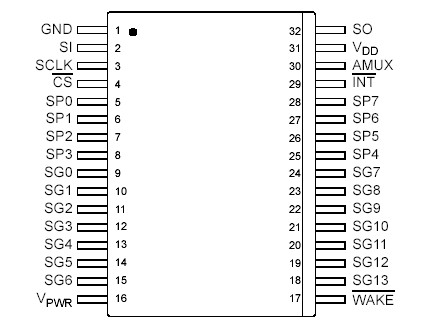
Pinout

  Connection Diagram


Specifications

Rating Symbol Value Unit
VDD Supply Voltage -0.3 to 7.0 VDC
CS , SI, SO, SCLK, INT, AMUX (Note 1) -0.3 to 7.0 VDC
WAKE  (Note 1) -0.3 to 40 VDC
VPWR Supply Voltage (Note 1) -0.3 to 50 VDC
Switch Input Voltage Range -14 to 40 VDC
Frequency of SPI Operation (VDD = 5.0 V) 6.0 MHz
ESD Voltage (Note 2)
Human Body Model (Note 3), (Note 4)
Machine Model (Note 5)
VESD1
VESD2
±4000
±200
V
Storage Temperature TSTG -55 to 150
Operating Case Temperature TC -40 to 125
Operating Junction Temperature TJ -40 to 150
Power Dissipation (TA = 25) (Note 6) PD 1.7 W
Thermal Resistance
Junction to Ambient
Junction to Lead
RJA
RJL
74
25
/W


Description

The 33993 Multiple Switch Detection Interface is designed to detect the closing and opening of up to 22 switch contacts. The switch status, either open or closed, is transferred to the microprocessor unit (MCU) through a serial peripheral interface (SPI). The device also features a 22-to-1 analog multiplexer for reading inputs as analog. The analog input signal is buffered and provided on the AMUX output pin for the MCU to read.

The 33993 device has two modes of operation, Sleep and Normal. The Sleep mode provides low quiescent current and enables the wake-up features of the device. Normal mode allows programming of the device and supplies switch contacts with pull-up or pull-down current as it monitors switch change of state.

The 33993 is packaged in the 32-pin wide-body SOIC, reducing circuit board area. Low quiescent current makes the 33993 ideal for automotive and industrial products requiring low sleep state currents. The internal block diagram of the 33993 is illustrated in Figure 1, page 2.


Customers Who Bought This Item Also Bought

Margin,quality,low-cost products with low minimum orders. Secure your online payments with SeekIC Buyer Protection.
RF and RFID
Power Supplies - External/Internal (Off-Board)
Industrial Controls, Meters
Integrated Circuits (ICs)
View more