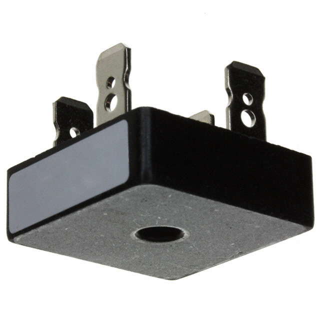
36Mb

Features: • 1M x 36 or 2M x 18.• On-chip delay-locked loop (DLL) for wide data valid window.• Common I/O read and write ports.• Synchronous pipeline read with late write operation.• Double data rate (DDR-II) interface for read and write input ports.• Fixed 4-bit...

product image

36Mb Picture
SeekIC No. : 004229068 Detail

36Mb: Features: • 1M x 36 or 2M x 18.• On-chip delay-locked loop (DLL) for wide data valid window.• Common I/O read and write ports.• Synchronous pipeline read with late write oper...

floor Price/Ceiling Price

Part Number:
36Mb
Supply Ability:
5000

Price Break

  • Qty
  • 1~5000
  • Unit Price
  • Negotiable
  • Processing time
  • 15 Days
Total Cost: $ 0.00

SeekIC Buyer Protection PLUS - newly updated for 2013!

  • Escrow Protection.
  • Guaranteed refunds.
  • Secure payments.
  • Learn more >>

Month Sales

268 Transactions

Rating

evaluate  (4.8 stars)

Upload time: 2024/4/25

Payment Methods

All payment methods are secure and covered by SeekIC Buyer Protection PLUS.

Notice: When you place an order, your payment is made to SeekIC and not to your seller. SeekIC only pays the seller after confirming you have received your order. We will also never share your payment details with your seller.
Product Details

Description


Features:

• 1M x 36 or 2M x 18.
• On-chip delay-locked loop (DLL) for wide data valid window.
• Common I/O read and write ports.
• Synchronous pipeline read with late write operation.
• Double data rate (DDR-II) interface for read and write input ports.
• Fixed 4-bit burst for read and write operations.
• Clock stop support.
• Two input clocks (K and K) for address and control registering at rising edges only.
• Two input clocks (C and C) for data output control.
• Two echo clocks (CQ and CQ) that are delivered simultaneously with data.
• +1.8V core power supply and 1.5, 1.8V VDDQ, used with 0.75, 0.9V VREF.
• HSTL input and output levels.
• Registered addresses, write and read controls, byte writes, and data outputs.
• Full data coherency.
• Boundary scan using limited set of JTAG 1149.1 functions.
• Byte write capability.
• Fine ball grid array (FBGA) package
- 15mm x 17mm body size
- 1mm pitch
- 165-ball (11 x 15) array
• Programmable impedance output drivers via 5x user-supplied precision resistor.


Specifications

Item
Symbol
Rating
Units
Power supply voltage
VDD
-0.5 to 2.6
V
Output power supply voltage
VDDQ
-0.5 to 2.6
V
Input voltage
VIN
-0.5 to 2.6
V
Data out voltage
VDOUT
-0.5 to 2.6
V
Operating temperature
TA
0 to 70
Junction temperature
TJ
110
Storage temperature
TSTG
-55 to +125
Note: Stresses greater than those listed in this table can cause permanent damage to the device. This is a stress rating only and functional operation of the device at these or any other conditions above those indicated in the operational sections of this datasheet is not implied. Exposure to absolute maximum rating conditions for extended periods may affect reliability.


Description

The 36Mb IS61DDB41M36 and IS61DDB42M18 are synchronous, high-performance CMOS static random access memory (SRAM) devices. These SRAMs have a common I/O bus. The rising edge of K clock initiates the read/write operation, and all internal operations are self-timed. Refer to the Timing Reference Diagram for Truth Table on p.8 for a description of the basic operations of these DDR-II (Burst of 4) CIO SRAMs.

Read and write addresses are registered on alternating rising edges of 36Mb. Reads and writes are performed in double data rate. The following are registered internally on the rising edge of the K clock:

• Read and write addresses
• Address load
• Read/write enable
• Byte writes for burst addresses 1 and 3
• Data-in for burst addresses 1 and 3 The following are registered on the rising edge of the K clock:
• Byte writes for burst addresses 2 and 4
• Data-in for burst addresses 2 and 4

Byte writes can change with the corresponding datain to enable or disable writes on a per-byte basis. An internal write buffer enables the data-ins to be registered one cycle later than the write address. The first data-in burst is clocked one cycle later than the write command signal, and the second burst is timed to the following rising edge of the K clock. Two full  clock cycles are required to complete a write operation.

During the burst read operation, at the first and third bursts the data-outs are updated from output registers off the second and fourth rising edges of the C clock (starting 1.5 cycles later). At the second and fourth bursts, the data-outs are updated with the third and fifth rising edges of the corresponding C clock (see page 9). The K and K clocks are used to time the data-outs whenever the C and C clocks are tied high.

Two full clock cycles are required to complete a read operation The device is operated with a single +1.8V power supply and is compatible with HSTL I/O interfaces.


Customers Who Bought This Item Also Bought

Margin,quality,low-cost products with low minimum orders. Secure your online payments with SeekIC Buyer Protection.
Connectors, Interconnects
Computers, Office - Components, Accessories
Industrial Controls, Meters
Hardware, Fasteners, Accessories
Circuit Protection
Memory Cards, Modules
View more