39S13620TQ-6

Features: • All signals fully synchronous to the positiv edge of the system clock• Programmable burst lengths: 1, 2, 4, 8 or full page• Burst data transfer in sequential or interleaved order• Burst read with single write• Programmable CAS latency: 2, 3• 8 column...

product image

39S13620TQ-6 Picture
SeekIC No. : 004229525 Detail

39S13620TQ-6: Features: • All signals fully synchronous to the positiv edge of the system clock• Programmable burst lengths: 1, 2, 4, 8 or full page• Burst data transfer in sequential or interle...

floor Price/Ceiling Price

Part Number:
39S13620TQ-6
Supply Ability:
5000

Price Break

  • Qty
  • 1~5000
  • Unit Price
  • Negotiable
  • Processing time
  • 15 Days
Total Cost: $ 0.00

SeekIC Buyer Protection PLUS - newly updated for 2013!

  • Escrow Protection.
  • Guaranteed refunds.
  • Secure payments.
  • Learn more >>

Month Sales

268 Transactions

Rating

evaluate  (4.8 stars)

Upload time: 2024/4/29

Payment Methods

All payment methods are secure and covered by SeekIC Buyer Protection PLUS.

Notice: When you place an order, your payment is made to SeekIC and not to your seller. SeekIC only pays the seller after confirming you have received your order. We will also never share your payment details with your seller.
Product Details

Description


Features:

• All signals fully synchronous to the positiv edge of the system clock
• Programmable burst lengths: 1, 2, 4, 8 or full page
• Burst data transfer in sequential or interleaved order
• Burst read with single write
• Programmable CAS latency: 2, 3
• 8 column block write and write-per-bit modes
• Independent byte operation via DQM 0 ¼ 3 interface
• Auto precharge and auto refresh modes
• 2k refresh cycles/32 ms
• LVTTL compatible I/O
• Hidden auto precharge for read bursts


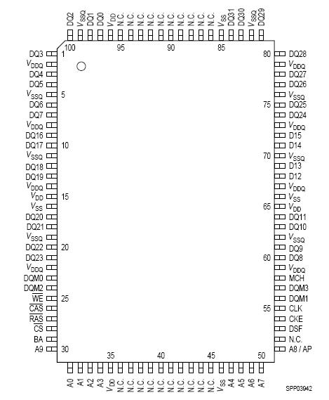
Pinout

  Connection Diagram


Specifications

Operating temperature range .......................................................................................0 to + 70 °C
Storage temperature range................................................................................... 55 to + 150 °C
Input/output voltage ......................................................................................... 0.3 to VDD + 0.3 V
Power supply voltage VDD/VDDQ............................................................................... 0.3 to + 4.6 V
Power Dissipation ....................................................................................................................... 1 W
Data out current (short circuit) ................................................................................................ 50 mA
Note: Stresses above those listed under "Absolute Maximum Ratings" may cause permanent
damage of the device. Exposure to absolute maximum rating conditions for extended
periods may affect device reliability.


Description

The HYB 39S13620TQ-6 are dual bank Synchronous Graphics DRAM's (SGRAM) organized as 2 banks256 Kbit´ 32 with built-in graphics features. These synchronous devices achieve high speed data transfer rates up to 143 MHz by employing a chip architecture that prefetches multiple bits and then synchronizes the output data to a system clock. The chip is fabricated with an advanced 64MBit DRAM process technology.

The 39S13620TQ-6 is designed to comply with all JEDEC standards set for synchronous graphics DRAM products, both electrically and mechanically.

RAS, CAS, WE, DSF and CS are pulsed signals which are examined at the positive edge of each externally applied clock. Internal chip operating modes are defined by combinations of these signals. A ten bit address bus accepts address data in the conventional RAS/CAS multiplexing style. Ten row address bits (A0 - A9) and a bank select BA are strobed with RAS. Column address bits plus a bank select are strobed with CAS.

Prior to any access operation, the CAS latency, burst length and burst sequence must be programmed into the device by address inputs during a mode register set cycle. An Auto Precharge function may be enabled to provide a self-timed row precharge. This is initiated at the end of the burst sequence. In addition, it features the write per bit, the block write and the masked block writefunctions. By having a programmable Mode register and Special Mode register, the system can select the best suitable modes to maximize its performance.

Operating the two memory banks in an interleave fashion allows random access operation to occur at higher rate than is possible with standard DRAMs. A sequential and gapless data rate of up to 143 MHz is possible depending on burst length, CAS latency and speed grade of the device. Auto Refresh (CBR) and Self Refresh operation are supported.

The 39S13620TQ-6 operates with a single 3.3 V±0.3 V power supply and are available in 100 pin TQFP package.


Customers Who Bought This Item Also Bought

Margin,quality,low-cost products with low minimum orders. Secure your online payments with SeekIC Buyer Protection.
Crystals and Oscillators
Motors, Solenoids, Driver Boards/Modules
Cable Assemblies
View more