Features: • Fast access times: 9, 10, and 12ns
• Fast clock speed: 66, and 50 MHz
• Provide high performance 2-1-1-1 access rate
• Fast OE# access times: 5 and 6ns
• Single +3.3V -5% and +10% power supply
• 5V tolerant inputs except I/O's
• Clamp diodes to VSSQ at all inputs and outputs
• Common data inputs and data outputs
• BYTE WRITE ENABLE and GLOBAL WRITE control
• Three chip enables for depth expansion and address ipeline
• Address, data and control registers
• Internally self-timed WRITE CYCLE
• Burst control pins (interleaved or linear burst sequence)
• Automatic power-down for portable applications
• High density, high speed packages
• Low capacitive bus loading
• High 30pF output drive capability at rated access timePinout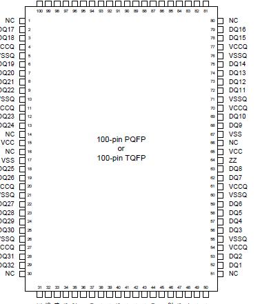 Specifications
Voltage on VCC Supply Relative to VSS. .-0.5V to +4.6V
VIN .........................................................-0.5V to VCC+0.5V
Storage Temperature (plastic) ....................-55oC to +125o
Junction Temperature ................................................+125o
Power Dissipation ........................................................1.4W
Short Circuit Output Current .....................................100mA
*Stresses greater than those listed under "Absolute MaximumRatings" may cause permanent damage to the device.This is a stressrating only and functional operation of the device at these or anyother conditions above those indicated in the operational sections ofthis specification is not implied. Exposure to absolute maximumrating conditions for extended periods may affect reliability.
DescriptionThe Galvantech Synchronous Burst SRAM family of 6523 employs high-speed, low power CMOS designs usingadvanced double-layer polysilicon, double-layer metaltechnology. Each memory cell consists of four transistors andtwo high valued resistors.
The 6523 SRAM integrates 65536 x18 SRAMcells with advanced synchronous peripheral circuitry and a 2-bit counter for internal burst operation. All synchronousinputs are gated by registers controlled by a positive-edgetriggeredclock input (CLK). The synchronous inputs includeall addresses, all data inputs, address-pipelining chip enable(CE#), depth-expansion chip enables (CE2# and CE2), burstcontrol inputs (ADSC#, ADSP#, and ADV#), write enables(WEL#, WEH#, and BWE#), and global write (GW#).Asynchronous inputs include the output enable (OE#),burst mode control (MODE), and sleep mode control (ZZ).The data outputs (DQ), enabled by OE#, are alsoasynchronous.
Addresses and chip enables of 6523 are registered with eitheraddress status processor (ADSP#) or address status controller(ADSC#) input pins. Subsequent burst addresses can beinternally generated as controlled by the burst advance pin(ADV#).
Address, data inputs, and write controls of 6523 are registered onchipto initiate self-timed WRITE cycle. WRITE cycles canbe one or two bytes wide as controlled by the write controlinputs. Individual byte enables allow individual bytes to bewritten. WEL# controls DQ1-DQ8 and DQP1. WEH#controls DQ9-DQ16 and DQP2. WEL# and WEH# can beactive only with BWE# being LOW. GW# being LOW causesall bytes to be written.
The 6523 operates from a +3.3V power supply.All inputs and outputs are TTL-compatible. The device isideally suited for 486, PentiumTM, 680x0, and PowerPCTMsystems and for systems that are benefited from a widesynchronous data bus.

 6523 Data Sheet