Features: ·Members of the Texas Instruments WidebusE Family
·Inputs Are TTL-Voltage Compatible
·3-State Outputs Drive Bus Lines Directly
·Provide Extra Bus Driving/Latches Necessary for Wider Address/Data Paths or Buses With Parity
·Flow-Through Architecture Optimizes PCB Layout
·Distributed VCC and GND Pin Configuration Minimizes High-Speed Switching Noise
·EPIC™ (Enhanced-Performance Implanted CMOS) 1-mm Process
·500-mA Typical Latch-Up Immunity at 125°C
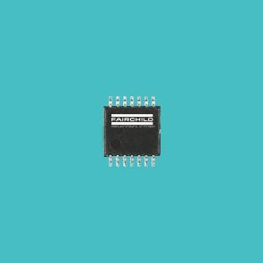
·Package Options Include Plastic Thin Shrink Small-Outline (DGG) Packages, 300-mil Shrink Small-Outline (DL) Packages Using 25-mil Center-to-Center Pin Spacings, and 380-mil Fine-Pitch Ceramic Flat (WD) Packages Using 25-mil Center-to-Center Pin SpacingsPinout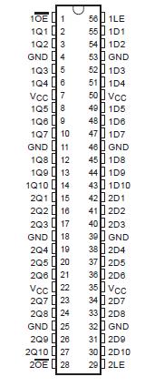 Specifications
Supply voltage range, VCC . . . . . . . . . . . . . . . . . . . . .. . . . . ... . .. . . . . . . . 0.5 V to 7 V
Input voltage range, VI (see Note 1) . . . . . . . . . . . . . . . . . . ... . . 0.5 V to VCC + 0.5 V
Output voltage range, VO (see Note 1) . . . . . . . . . .. . . . . . . ... . . 0.5 V to VCC + 0.5 V
Input clamp current, IIK (VI < 0 or VI > VCC) . . . . . . . . . . . . . . . . . . . .. ... . . . . . ±20 mA
Output clamp current, IOK (VO < 0 or VO > VCC) . . . . . . . . . . . . . . .. . . .... . . . . . ±50 mA
Continuous output current, IO (VO = 0 to VCC) . . . . . . . . . . . . . . . .. .... . . . . . . . ±50 mA
Continuous current through VCC or GND . . . . . . . . . . . . . . . . . . . . . . . . . . . . . . ±400 mA
Maximum power dissipation at TA = 55°C (in still air) (see Note 2): DGG package . . 1 W
DL package . . . . . .. . . .. . . .. . . .. . . .. . . .. . . .. . . .. . . .. . . .. . . .. . . .. . . .. . . . . . . . 1.4 W
Storage temperature range, Tstg . . . . . . . . . . . . . . . . . . . . . . . . .. . . . . 65°C to 150°C
† Stresses beyond those listed under "absolute maximum ratings" may cause permanent damage to the device. These are stress ratings only, andfunctional operation of the device at these or any other conditions beyond those indicated under "recommended operating conditions" is notimplied. Exposure to absolute-maximum-rated conditions for extended periods may affect device reliability.
NOTES: 1. The input and output voltage ratings may be exceeded if the input and output current ratings are observed.
2. The maximum package power dissipation is calculated using a junction temperature of 150 and a board trace length of 750 mils.
DescriptionThese 20-bit latches feature of the 74ACT16841 3-state outputs designed specifically for driving highly capacitive or relatively low-impedance loads. They are particularly suitable for implementing buffer registers, I/O ports, bidirectional bus drivers, and working registers.
The 74ACT16841 can be used as two 10-bit latches or one 20-bit latch. The 20 latches are transparent D-type. While the latch-enable (1LE or 2LE) input is high, the Q outputs of the corresponding 10-bit latch follow the data (D) inputs. When LE is taken low, the Q outputs are latched at the levels that were set up at the D inputs.
A buffered output-enable (1OE or 2OE) input can be used to place the outputs of the corresponding 10-bit latch in either a normal logic state (high or low logic levels) or a high-impedance state. In the high-impedance state, the outputs neither load nor drive the bus lines significantly.
OE does not affect the internal operation of the latches. Old data can be retained or new data can be entered while the outputs are in the high-impedance state.

 74ACT16841 Data Sheet