74HC2G125

Features: · Wide supply voltage range from 2.0 to 6.0 V· Symmetrical output impedance· High noise immunity· Low power dissipation· Balanced propagation delays· Very small 8 pins package· Output capability: bus driver· ESD protection: HBM EIA/JESD22-A114-A exceeds 2000 V MM EIA/JESD22-A115-A exceed...

product image

74HC2G125 Picture
SeekIC No. : 004250741 Detail

74HC2G125: Features: · Wide supply voltage range from 2.0 to 6.0 V· Symmetrical output impedance· High noise immunity· Low power dissipation· Balanced propagation delays· Very small 8 pins package· Output capa...

floor Price/Ceiling Price

Part Number:
74HC2G125
Supply Ability:
5000

Price Break

  • Qty
  • 1~5000
  • Unit Price
  • Negotiable
  • Processing time
  • 15 Days
Total Cost: $ 0.00

SeekIC Buyer Protection PLUS - newly updated for 2013!

  • Escrow Protection.
  • Guaranteed refunds.
  • Secure payments.
  • Learn more >>

Month Sales

268 Transactions

Rating

evaluate  (4.8 stars)

Upload time: 2024/4/28

Payment Methods

All payment methods are secure and covered by SeekIC Buyer Protection PLUS.

Notice: When you place an order, your payment is made to SeekIC and not to your seller. SeekIC only pays the seller after confirming you have received your order. We will also never share your payment details with your seller.
Product Details

Description


Features:

· Wide supply voltage range from 2.0 to 6.0 V
· Symmetrical output impedance
· High noise immunity
· Low power dissipation
· Balanced propagation delays
· Very small 8 pins package
· Output capability: bus driver
· ESD protection:
  HBM EIA/JESD22-A114-A exceeds 2000 V
  MM EIA/JESD22-A115-A exceeds 200 V.
· Specified from -40 to +85 °C and -40 to +125 °C.


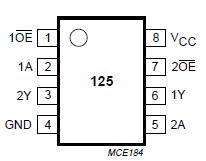
Pinout

  Connection Diagram


Specifications

SYMBOL PARAMETER CONDITIONS MIN. MAX. UNIT
VCC supply voltage   -0.5 +7.0 V
IIK input diode current VI < -0.5 V or VI > VCC + 0.5 V ;note 1 - ±20 mA
IOK output diode current VO < -0.5 V or VO > VCC + 0.5 V ;note 1 - ±20 mA
IO output source or sink current -0.5 V < VO < VCC + 0.5 V ;note 1 - 25 mA
ICC VCC or GND current note 1 - 50 mA
Tstg storage temperature   -65 +150 °C
PD power dissipation per package for temperature range from -40 to +125 °C; note 2 - 300 mW
Notes
1. The input and output voltage ratings may be exceeded if the input and output current ratings are observed.
2. Above 110 °C the value of PDderates linearly with 8 mW/K.


Description

The 74HC2G125 is a high-speed Si-gate CMOS device.

The 74HC2G125 provides one non-inverting buffer/line driver with 3-state output. The 3-state output is controlled by the output enable input pin (OE). A HIGH at pin OE causes the output to assume a high-impedance OFF-state.

The bus driver output currents are equal compared to the 74HC2G125.


Customers Who Bought This Item Also Bought

Margin,quality,low-cost products with low minimum orders. Secure your online payments with SeekIC Buyer Protection.
Boxes, Enclosures, Racks
Test Equipment
Audio Products
Sensors, Transducers
Line Protection, Backups
View more