74HCT112

Features: · Asynchronous set and reset· Output capability: standard· ICC category: flip-flopsPinoutDescriptionThe 74HCT112 is designed as high-speed si-gate CMOS devices and are pin compatible with low power schottky TTL (LSTTL). It is specified in compliance with JEDEC standard no. 7A which is du...

product image

74HCT112 Picture
SeekIC No. : 004250812 Detail

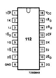
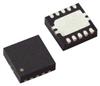
74HCT112: Features: · Asynchronous set and reset· Output capability: standard· ICC category: flip-flopsPinoutDescriptionThe 74HCT112 is designed as high-speed si-gate CMOS devices and are pin compatible with ...

floor Price/Ceiling Price

Part Number:
74HCT112
Supply Ability:
5000

Price Break

  • Qty
  • 1~5000
  • Unit Price
  • Negotiable
  • Processing time
  • 15 Days
Total Cost: $ 0.00

SeekIC Buyer Protection PLUS - newly updated for 2013!

  • Escrow Protection.
  • Guaranteed refunds.
  • Secure payments.
  • Learn more >>

Month Sales

268 Transactions

Rating

evaluate  (4.8 stars)

Upload time: 2024/5/3

Payment Methods

All payment methods are secure and covered by SeekIC Buyer Protection PLUS.

Notice: When you place an order, your payment is made to SeekIC and not to your seller. SeekIC only pays the seller after confirming you have received your order. We will also never share your payment details with your seller.
Product Details

Description


Features:

· Asynchronous set and reset
· Output capability: standard
· ICC category: flip-flops


Pinout

  Connection Diagram


Description

The 74HCT112 is designed as high-speed si-gate CMOS devices and are pin compatible with low power schottky TTL (LSTTL). It is specified in compliance with JEDEC standard no. 7A which is dual negative-edge triggered JK-type flip-flops featuring individual nJ, nK, clock (nCP), set (nSD) and reset (nRD) inputs.

The three features of the 74HCT112. The first one is asynchronous set and reset. The second one is its output capability would be standard. The third one is its ICC category would be flip-flops. That are all the main features.

Some important AC characteristics and specifications of the 74HCT112 have been concluded into several points as follow.For Tamb=25°C the first one is about its propagation delay which would be typ 55ns and max 175ns at Vcc=2.0V and would be typ 20ns and max 35ns at Vcc=4.5V and would be typ 16ns and max 30ns at Vcc=6.0V. The second one is about its output transition time which would be typ 19ns and max 75ns at Vcc=2.0V and typ 7ns and max 15ns at Vcc=4.5V and would be typ 6ns and max 13ns at Vcc=6.0V. The third one is about its clock pulse width which would be min 80ns and typ 22ns at Vcc=2.0V and min 16ns and typ 8ns at Vcc=4.5V and would be min 14ns and typ 6ns at Vcc=6.0V. The fourth one is about its set or reset pulse width low which would be min 80ns and typ 22ns at Vcc=2.0V and min 16ns and typ 8ns at Vcc=4.5V and would be min 14ns and typ 6ns at Vcc=6.0V.

Also for the Tamb range of the 74HCT112 -40 to +125°C the first one is about its propagation delay which would be max 265ns at Vcc=2.0V and would be max 53ns at Vcc=4.5V and would be max 45ns at Vcc=6.0V. The second one is about its output transition time which would be max 110ns at Vcc=2.0V and max 22ns at Vcc=4.5V and would be max 19ns at Vcc=6.0V. The third one is about its clock pulse width which would be min 120ns at Vcc=2.0V and min 24ns at Vcc=4.5V and would be min 20ns at Vcc=6.0V. The fourth one is about its output transition time which would be min 120ns at Vcc=2.0V and min 24ns at Vcc=4.5V and would be min 20ns at Vcc=6.0V. And so on. For more information please contact us.


The 74HCT112 are high-speed Si-gate CMOS devices and are pin compatible with low power Schottky TTL (LSTTL). They are specified in compliance with JEDEC standard no. 7A.

The 74HCT112 are dual negative-edge triggered JK-type flip-flops featuring individual nJ, nK, clock (nCP), set (nSD) and reset (nRD) inputs.

The set and reset inputs, when LOW, set or reset the outputs as shown in the function table regardless of the levels at the other inputs.

A HIGH level at the clock (nCP) input enables the nJ and nK inputs and data will be accepted. The nJ and nK inputs control the state changes of the flip-flops as shown in the function table. The nJ and nK inputs must be stable one set-up time prior to the HIGH-to-LOW clock transition for predictable operation.

Output state changes are initiated by the HIGH-to-LOW transition of nCP.

Schmitt-trigger action of the 74HCT112 in the clock input makes the circuit highly tolerant to slower clock rise and fall times.


Customers Who Bought This Item Also Bought

Margin,quality,low-cost products with low minimum orders. Secure your online payments with SeekIC Buyer Protection.
Computers, Office - Components, Accessories
Fans, Thermal Management
Integrated Circuits (ICs)
Resistors
RF and RFID
View more