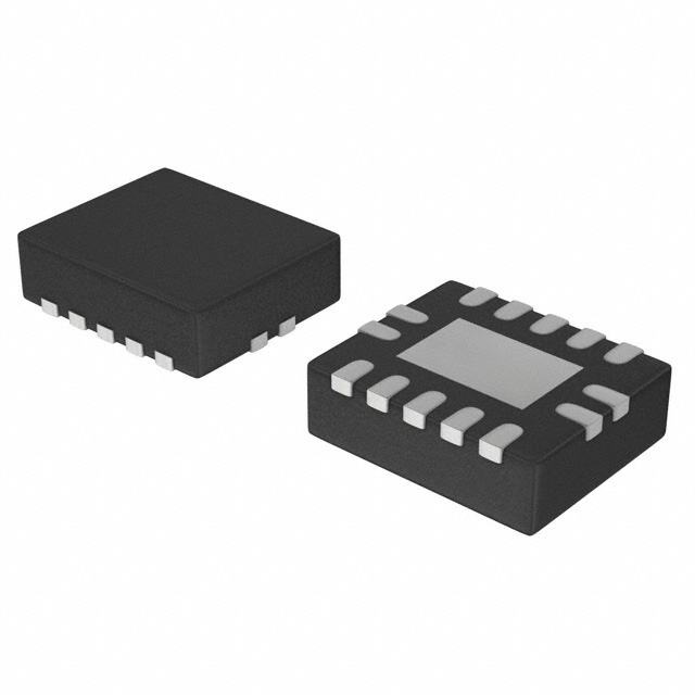
DescriptionThe 74LV123N belongs to 74LV123 family which is a low-voltage Si-gate CMOS device and is pin and function compatible with the 74HC/HCT123. The 74LV123 is a dual retriggerable monostable multivibrator with output pulse width control by three methods. The basic pulse time is programmed by selection of an external resistor (REXT) and capacitor (CEXT). They are normally connected as shown in Figure 1. Once triggered, the basic output pulse width may be extended by retriggering the gated active LOW-going edge input (nA) or the active HIGH-going edge input (nB). By repeating this process, the output pulse period (nQ = HIGH, nQ = LOW) can be made as long as desired. Alternatively, an output delay can be terminated at any time by a LOW-going edge on input nRD, which also inhibits the triggering. Figures 1 and 2 illustrate pulse control by retriggering and early reset. The basic output pulse width of the 74LV123N is essentially determined by the values of the external timing components REXT and CEXT. For pulse width when CEXT <10000pF, see Figure 5. When CEXT > 10,000pF, the typical output pulse width is defined as: tW = 0.45 * REXT * CEXT (typ.), where tW = pulse width in ns; REXT = external resistor in K; and CEXT = external capacitor in pF. Schmitt-trigger action in the nA and nB inputs makes the circuit highly tolerant of slower input rise and fall times.
The features of 74LV123N can be summarized as (1)optimized for Low Voltage applications: 1.0 to 5.5V; (2)accepts TTL input levels between VCC = 2.7V and VCC = 3.6V; (3)typical VOLP (output ground bounce) < 0.8V @ VCC = 3.3V, Tamb = 25°C; (4)typical VOHV (output VOH undershoot) > 2V @ VCC = 3.3V, Tamb = 25°C; (5)DC triggered from active HIGH or active LOW inputs; (6)retriggerable for very long pulses up to 100% duty factor; (7)direct reset terminates output pulses; (8)schmitt-trigger action on all inputs except for the reset input; (9)output capability: standard (except for nREXT/CEXT); (10)ICC category: MSI.
The absolute maximum ratings of 74LV123N are (1)VCC DC supply voltage: -0.5 to +7.0 V; (2)±IIK DC input diode current(VI < -0.5 or VI > VCC + 0.5V): 20mA; (3)±IOK DC output diode current(VO < -0.5 or VO > VCC + 0.5V): 50mA; (4)±IO DC output source or sink current - standard outputs(-0.5V < VO < VCC + 0.5V): 25mA; (5)±IGND, ±ICC DC VCC or GND current for types with - standard outputs: 50mA; (6)Tstg storage temperature range: -65 to +150 °C; (7)PTOT power dissipation per package for temperature range of the 74LV123N: -40 to +125°C-plastic DIL(above +70°C derate linearly with 12mW/K)/-plastic mini-pack (SO)(above +70°C derate linearly with 8 mW/K)/-plastic shrink mini-pack (SSOP and TSSOP)(above +60°C derate linearly with 5.5 mW/K): 750/500/500mW.(1. Stresses beyond those listed may cause permanent damage to the device. These are stress ratings only and functional operation of the 74LV123N at these or any other conditions beyond those indicated under arecommended operating conditions is not implied. Exposure to absolute-maximum-rated conditions for extended periods may affect device reliability. 2. The input and output voltage ratings may be exceeded if the input and output current ratings are observed.)

 74LV123N Data Sheet


