Features: Wide supply voltage range from 1.65 V to 5.5 V
5 V tolerant input/output for interfacing with 5 V logic
High noise immunity
Complies with JEDEC standard:
JESD8-7 (1.65 V to 1.95 V)
JESD8-5 (2.3 V to 2.7 V)
JESD8-B/JESD36 (2.7 V to 3.6 V).
ESD protection:
HBM EIA/JESD22-A114-B exceeds 2000 V
MM EIA/JESD22-A115-A exceeds 200 V.
-24 mA output drive (VCC = 3.0 V)
CMOS low power consumption
Latch-up performance exceeds 250 mA
Direct interface with TTL levels
Inputs accept voltages up to 5 V
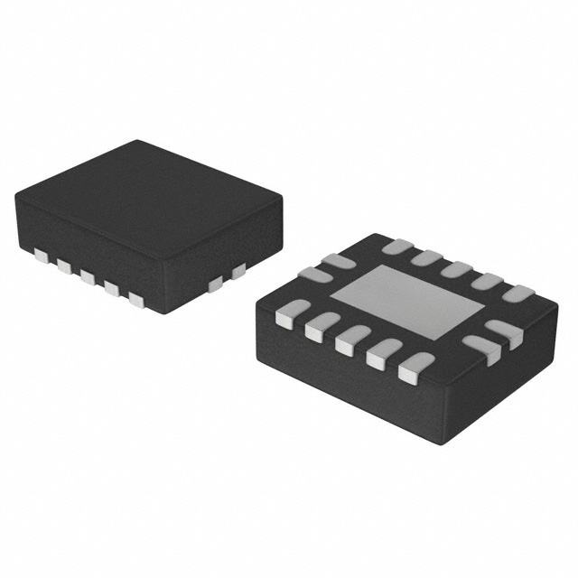
Multiple package options
Specified from -40 °C to +85 °C and -40 °C to +125 °C.Pinout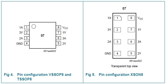 Specifications
| SYMBOL |
PARAMETER |
CONDITIONS |
MIN. |
MAX. |
UNIT |
| VCC |
supply voltage |
|
-0.5 |
+6.5 |
V |
| VI |
input voltage |
[1] |
-0.5 |
+6.5 |
V |
| VO |
output voltage |
active mode [1] |
-0.5 |
+6.5 |
V |
| Power-down mode[1] [2] |
-0.5 |
+6.5 |
V |
| IIK |
input diode current |
VI< 0 V |
- |
-50 |
mA |
| IOK |
output diode current |
VO< 0 V |
- |
-50 |
mA |
| IO |
output source or sink current |
VO = 0 V to 6.5 V |
- |
50 |
mA |
| ICC, IGND |
VCC or GND current |
|
- |
±100 |
mA |
| Tstg |
storage temperature |
|
-65 |
+150 |
°C |
| Ptot |
power dissipation |
Tamb = -40 °C to +125 °C |
- |
300 |
mW |
[1] The input and output voltage ratings may be exceeded if the input and output current ratings are observed.
[2] When VCC = 0 V (Power-down mode), the output voltage can be 5.5 V in normal operation.DescriptionThe 74LVC3G07 is a high-performance, low-power, low-voltage, Si-gate CMOS device and superior to most advanced CMOS compatible TTL families.
Input can be driven from either 3.3 V or 5 V devices. This feature allows the use of this device in a mixed 3.3 V and 5 V environment.
Schmitt trigger action at all inputs makes the circuit tolerant for slower input rise and fall time.
The 74LVC3G07 is fully specified for partial power-down applications using I
off . The I
off circuitry disables the output, preventing the damaging backflow current through the device when it is powered down.
The 74LVC3G07 provides three non-inverting buffers.
The output of the device is an open drain and can be connected to other open-drain outputs to implement active-LOW wired-OR or active-HIGH wired-AND functions.

 74LVC3G07 Data Sheet