82434LX

Features: Supports the PentiumTMProcessor at iCOMP TM Index 510T60 MHz and iCOMP Index 567T66 MHzSupports the Pentium Processor at iCOMP Index 735T90 MHz iCOMP Index 815T100 MHz and iCOMP Index 610T75MHzSupports Pipelined Addressing Capability of the Pentium ProcessorThe 82430NX Drives 33V Signal ...

product image

82434LX Picture
SeekIC No. : 004255568 Detail

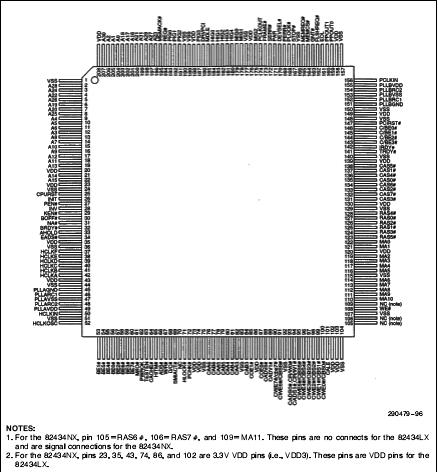
82434LX: Features: Supports the PentiumTMProcessor at iCOMP TM Index 510T60 MHz and iCOMP Index 567T66 MHzSupports the Pentium Processor at iCOMP Index 735T90 MHz iCOMP Index 815T100 MHz and iCOMP Index 610T...

floor Price/Ceiling Price

Part Number:
82434LX
Supply Ability:
5000

Price Break

  • Qty
  • 1~5000
  • Unit Price
  • Negotiable
  • Processing time
  • 15 Days
Total Cost: $ 0.00

SeekIC Buyer Protection PLUS - newly updated for 2013!

  • Escrow Protection.
  • Guaranteed refunds.
  • Secure payments.
  • Learn more >>

Month Sales

268 Transactions

Rating

evaluate  (4.8 stars)

Upload time: 2024/4/26

Payment Methods

All payment methods are secure and covered by SeekIC Buyer Protection PLUS.

Notice: When you place an order, your payment is made to SeekIC and not to your seller. SeekIC only pays the seller after confirming you have received your order. We will also never share your payment details with your seller.
Product Details

Description


Features:

Supports the PentiumTMProcessor at iCOMP TM Index 510T60 MHz and iCOMP Index 567T66 MHz
Supports the Pentium Processor at iCOMP Index 735T90 MHz iCOMP Index 815T100 MHz and iCOMP Index 610T75
MHz
Supports Pipelined Addressing Capability of the Pentium Processor
The 82430NX Drives 33V Signal Levels on the CPU and Cache Interfaces
High Performance CPUPCIMemory Interfaces via Posted Write and Read Prefetch Buffers
Fully Synchronous PCI Interface with Full Bus Master Capability
Supports the Pentium Processor Internal Cache in Either Write-Through or Write-Back Mode
Programmable Attribute Map of DOS and BIOS Regions for System Flexibility
Integrated Low Skew Clock Driver for Distributing Host Clock
Integrated Second Level Cache Controller
Integrated Cache Tag RAM
   --Write-Through and Write-Back Cache Modes for the 82434LX
   --Write-Back for the 82434NX
   --82434NX Supports Low-Power Cache Standby
   --Direct Mapped Organization
   --Supports Standard and Burst SRAMs
   --256-KByte and 512-KByte Sizes
   --Cache Hit Cycle of 3-1-1-1 on Reads and Writes Using Burst SRAMs
   --Cache Hit Cycle of 3-2-2-2 on Reads and 4-2-2-2 on Writes Using Standard SRAMs
Integrated DRAM Controller
   --Supports 2 MBytes to 192 MBytes of Cacheable Main Memory for the 82434LX
   --Supports 2 MBytes to 512 MBytes of Cacheable Main Memory for the 82434NX
   --Supports DRAM Access Times of 70 ns and 60 ns
   --CPU Writes Posted to DRAM 4-1-1-1
   --Refresh Cycles Decoupled from ISA Refresh to Reduce the DRAM Access Latency
   --Six RAS Lines (82434LX)
   --Eight RAS Lines (82434NX)
   --Refresh by RAS-Only or CAS-Before-RAS in Single or Burst of Four
HostPCI Bridge
   --Translates CPU Cycles into PCI Bus Cycles
   --Translates Back-to-Back Sequential CPU Memory Writes into PCI Burst Cycles
   --Burst Mode Writes to PCI in Zero PCI Wait-States (ie Data Transfer EveryCycle)
   --Full Concurrency Between CPU-to-Main Memory and PCI-to-PCI Transactions
   --Full Concurrency Between CPU-to-Second Level Cache and PCI-to-Main Memory Transactions
   --Same Cache and Memory System Logic Design for ISA and EISA Systems
   --Cache Snoop Filter Ensures Data Consistency for PCI-to-Main Memory Transactions
208-Pin QFP Package


Pinout

  Connection Diagram


Specifications

Case TemperatureunderBias................ ........0to +85
Storage Temperature ..............................-55to +150
Voltage on Any Pin
    with RespecttoGround .....................-0.3 toVCC +0.3V
Supply Voltage
    with RespecttoVSS ................................-0.3 to +6.5V
Maximum TotalPower Dissipation ...........................2.0W
Maximum PowerDissipationVCC3 ........................470mW

The Maximum total power dissipation in the 82434NX on the VCC and VCC3 pins is 20W The VCC3 pins may draw as much as 470 mW however total power will not exceed 20W


Description

This document describes both the 82434LX and 82434NX Unshaded areas describe the 82434LX Shaded areas like this one describe 82434NX operations that differ from the 82434LX

The 82434LX82434NX PCI Cache Memory Controllers (PCMC) integrate the cache and main memory DRAM control functions and provide bus control for transfers between the CPU cache main memory and the PCI Local Bus The cache controller supports write-back (or write-through for 82434LX) cache policy and cache sizes of 256-KBytes and 512-KBytes The cache memory can be implemented with either standard or burst SRAMs The PCMC cache controller integrates a high-performance Tag RAM to reduce system cost


Customers Who Bought This Item Also Bought

Margin,quality,low-cost products with low minimum orders. Secure your online payments with SeekIC Buyer Protection.
Soldering, Desoldering, Rework Products
LED Products
Audio Products
RF and RFID
Cables, Wires - Management
View more