SeekIC No. : 004260033
Detail
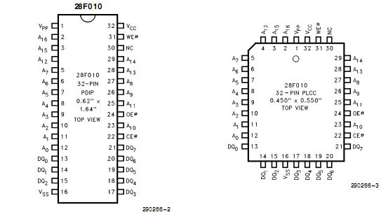
A28F010: Features: Automotive Temperature Range:-40§Cto a125§CFlash Memory Electrical Chip-Erase1 Second Typical Chip-EraseQuick-Pulse Programming Algorithm10 ms Typical Byte-Program2 Second Chip-Program1,00...
 A28F010 Data Sheet
floor Price/Ceiling Price
- Part Number:
- A28F010
- Supply Ability:
- 5000
Price Break
- Qty
- 1~5000
- Unit Price
- Negotiable
- Processing time
- 15 Days
SeekIC Buyer Protection PLUS - newly updated for 2013!
- Escrow Protection.
- Guaranteed refunds.
- Secure payments.
- Learn more >>
Month Sales
268 Transactions
Payment Methods
All payment methods are secure and covered by SeekIC Buyer Protection PLUS.
Notice: When you place an order, your payment is made to SeekIC and not to your seller. SeekIC only pays the seller after confirming you have received your order. We will also never share your payment details with your seller.