Features: ·5.0V ± 10% for read and write operations
· Access times:
- 55/70/90 (max.)
·Current:
- 20 mA typical active read current
- 30 mA typical program/erase current
- 1 mA typical CMOS standby
· Flexible sector architecture
- 8 Kbyte/ 4 KbyteX2/ 16 Kbyte/ 32 KbyteX3 sectors
- Any combination of sectors can be erased
- Supports full chip erase
- Sector protection:
A hardware method of protecting sectors to prevent
any inadvertent program or erase operations within
that sector
·Top or bottom boot block configurations available
·Embedded Erase Algorithms
- Embedded Erase algorithm will automatically erase the
entire chip or any combination of designated sectors
and verify the erased sectors
- Embedded Program algorithm automatically writes and
verifies bytes at specified addresses
·Typical 100,000 program/erase cycles per sector
·20-year data retention at 125°C
- Reliable operation for the life of the system
·Compatible with JEDEC-standards
- Pinout and software compatible with single-powersupply
Flash memory standard
- Superior inadvertent write protection
·Data Polling and toggle bits
- Provides a software method of detecting completion of
program or erase operations
·Erase Suspend/Erase Resume
- Suspends a sector erase operation to read data from,
or program data to, a non-erasing sector, then
resumes the erase operation
·Hardware reset pin (RESET )
- Hardware method to reset the device to reading array
data (not available on A290011)
·Package options
- 32-pin P-DIP, PLCC, or TSOP (Forward type)Pinout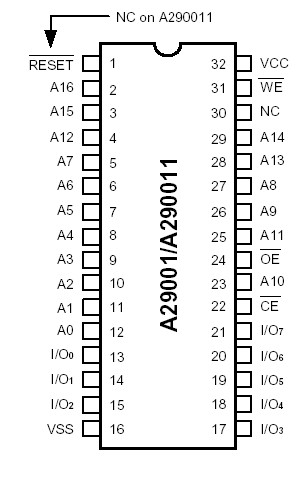 Specifications
Ambient Operating Temperature . . . . .. -55°C to + 125°C
Storage Temperature . . . . . . . . . . . . . . -65°C to + 125°C
Ground to VCC . . . . . . . . . . . . . . . . . . . ...... . . -2.0V to 7.0V
Output Voltage (Note 1) . . . . . . . . . . . . . ..... . -2.0V to 7.0V
A9, OE & RESET (Note 2) . . . . . . . .......... . . . -2.0V to 12.5V
All other pins (Note 1) . . . . . . . . . . . . . . . .... . -2.0V to 7.0V
Output Short Circuit Current (Note 3) . . . . ... . . . . . 200mA
Notes:
1. Minimum DC voltage on input or I/O pins is -0.5V. During voltage transitions, inputs may undershoot VSS to -2.0V for periods of up to 20ns. Maximum DC voltage on output and I/O pins is VCC +0.5V. During voltage transitions, outputs may overshoot to VCC +2.0V for periods up to 20ns.
2. Minimum DC input voltage on A9 pins is -0.5V. During voltage transitions, A9,OE and RESET may overshoot VSS to -2.0V for periods of up to 20ns. Maximum DC input voltage on A9 and OE is +12.5V which may overshoot to 13.5V for periods up to 20ns. (RESET is N/A on A290021)
3. No more than one output is shorted at a time. Duration of the short circuit should not be greater than one second.
DescriptionThe A29001 is a 5.0 volt-only Flash memory organized as 131,072 bytes of 8 bits each. The A29001 offers theRESET function, but it is not available on A290011. The 128 Kbytes of data are further divided into seven sectors for flexible sector erase capability. The 8 bits of data appear on I/O0 - I/O7 while the addresses are input on A0 to A16. The A29001 is offered in 32-pin PLCC, TSOP, and PDIP packages. This device is designed to be programmed in-system with the standard system 5.0 volt VCC supply. Additional 12.0 volt VPP is not required for in-system write or erase operations. However, the A29001 can also be programmed in standard EPROM programmers.
The A29001 has the first toggle bit, I/O6, which indicates whether an Embedded Program or Erase is in progress, or it is in the Erase Suspend. Besides the I/O6 toggle bit, the A29001 has a second toggle bit, I/O2, to indicate whether the addressed sector is being selected for erase. The A29001 also offers the ability to program in the Erase Suspend mode. The standard A29001 offers access times of 55, 70 and 90 ns allowing high-speed microprocessors to operate without wait states. To eliminate bus contention the device has separate chip enable (CE ), write enable (WE ) and output enable (OE ) controls.
The device A290011 requires only a single 5.0 volt power supply for both read and write functions. Internally generated and regulated voltages are provided for the program and erase operations. The A29001 is entirely software command set compatible with the JEDEC single-power-supply Flash standard. Commands are written to the command register using standard microprocessor write timings. Register contents serve as input to an internal state-machine that controls the erase and programming circuitry. Write cycles also internally latch addresses and data needed for the programming and erase operations. Reading data out of the device is similar to reading from other Flash or EPROM devices.
Device A290011 programming occurs by writing the proper program command sequence. This initiates the Embedded Program algorithm - an internal algorithm that automatically times the program pulse widths and verifies proper program margin. Device erasure occurs by executing the proper erase command sequence. This initiates the Embedded Erase algorithm - an internal algorithm that automatically preprograms the array (if it is not already programmed) before executing the erase operation. During erase, the device automatically times the erase pulse widths and verifies proper erase margin.

 A290011 Data Sheet