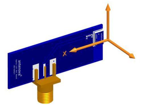
Bandwidth
:
Frequency
: 2.4 GHz
Technology Type
: Internal SMD Chip Antenna
Dimensions
: 6.1 mm L x 3.9 mm W x 1.1 mm H
Features: `Highly accurate 5 V, 100 mA guaranteed output
`Low dropout voltage, typically 380 mV at 100 mA
`Low quiescent current, typically 175 A
`Standby mode, maximum current 340 A (with 100 A load on OUTPUT)
`Unregulated DC input can withstand 20 V reverse battery and + 60 V power transients
`Fully operational for unregulated DC input voltage up to 26 V and regulated output voltage down to 3.0 V
`Reset output guaranteed for regulated output voltage down to 1.2 V
`No reverse output current
`Very low temperature coefficient for the regulated output
`Current limiting
`Comparator for voltage monitoring,voltage reference 1.52 V
`Programmable reset voltage monitoring
`Programmable power on reset (POR ) delay
`Watchdog with programmable time windows guarantees a minimum time and a maximum time between software clearing of the watchdog
`Time base accuracy ± 10%
`System enable output offers added security
`TTL/CMOS compatible
`-40 to +85 °C temperature range
`On request extended temperature range,-40 to +125 °C
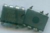
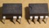
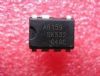
`DIP8 and SO8 packages
Application·Automotive systems
·Cellular telephones
·Security systems
·Battery powered products
·High efficiency linear power supplies
·Automotive electronicsPinout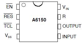 Specifications
| Parameter |
Symbol |
Conditions |
Continuous voltage at INPUT
to VSS |
VINPUT |
-0.3 to + 30 V |
Transients on INPUT for
t < 100 ms and duty cycle 1% |
VTRANS |
up to + 60 V |
| Reverse supply voltage on INPUT |
VREV |
- 20 V |
| Max. voltage at any signal pin |
VMAX |
OUTPUT + 0.3 V |
| Min. voltage at any signal pin |
VMIN |
VSS 0.3 V |
| Storage temperature |
TSTO |
-65 to + 150 °C |
| Electrostatic discharge max. to |
|
|
| MIL-STD-883C method 3015 |
VSmax |
1000 V |
| Max. soldering conditions |
TSmax |
250 °C x 10 s |
Stresses above these listed maximum ratings may cause permanent damage to the device. Exposure beyondspecified operating conditions may affect device reliability or cause malfunction.
DescriptionThe A6150 offers a high level of integration by combining voltage regulation, voltage monitoring and software monitoring in an 8 lead package. The voltage regulator has a low dropout voltage (typ. 380 mV at 100 mA) and a low quiescent current (175 A). The quiescent current increases only slightly in dropout prolonging battery life. Built-in protection includes a positive transient absorber for up to 60 V (load dump) and the ability to survive an unregulated input voltage of 20 V (reverse battery). The input may be connected to ground or a reverse voltage without reverse current flow from the output to the input. A comparator monitors the voltage applied at the VIN input comparing it with an internal 1.52 V reference. The poweron reset function is initialized after VIN reaches 1.52 V and takes the reset output inactive after TPOR depending of external resistance. The reset output goes active low when the VIN voltage is less than 1.52 V. The RES and EN outputs are guaranteed to be in a correct state for a regulated output voltage as low as 1.2 V. The watchdog function monitors software cycle time and execution. If software clears the watchdog too quickly (incorrect cycle time) or too slowly (incorrect execution) it will cause the system to be reset. The system enable output prevents critical control functions being activated until software has successfully cleared the watchdog three times. Such a security could be used to prevent motor controls being energized on repeated resets of a faulty system.
Parameters: | Technical/Catalog Information | A6150 |
| Vendor | Antenova (VA) |
| Category | RF and RFID |
| Frequency | 2.4GHz ~ 2.5GHz |
| Number of Bands | Single |
| Mounting Type | Surface Mount |
| Packaging | Cut Tape (CT) |
| VSWR | 1.9 |
| Antenna Type | Chip |
| Height (Max) | 0.04" (1.25mm) |
| Termination | Chip |
| Gain | 0.2dBi |
| Lead Free Status | Lead Free |
| RoHS Status | RoHS Compliant |
| Other Names | A6150
A6150
627 1013 1 ND
62710131ND
627-1013-1
|
 A6150 Data Sheet