Features: ·Two Matched ADCs with Input Signal Conditioning
·Selectable Bipolar Input Voltage Range (60.5 V, 61.0 V, 62.0 V)
·Full MIL-STD-883B Compliant
·80 dB Spurious-Free Dynamic Range
·Trimmed Channel-Channel MatchingApplication·Radar Processing
·Communications Receivers
·FLIR Processing
·Secure Communications
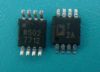
·Any I/Q Signal Processing ApplicationPinout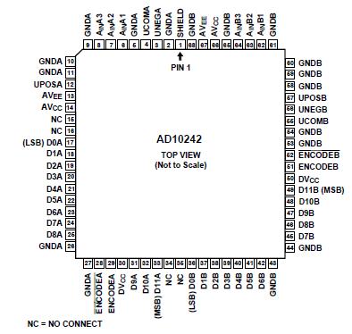
 Specifications
|
Parameter |
Min |
Max |
Units |
| ELECTRICAL |
| VCC Voltage |
0 |
7 |
V |
| VEE Voltage |
-7 |
0 |
V |
| Analog Input Voltage |
VEE |
VCC |
V |
| Analog Input Current |
-10 |
+10 |
mA |
| Digital Input Voltage (ENCODE) |
0 |
VCC |
V |
| ENCODE,ENCODE Differential Voltage |
|
4 |
V |
| Digital Output Current |
-40 |
+40 |
mA |
| ENVIRONMENTAL2 |
| Operating Temperature (Case) |
-55 |
+125 |
°C |
| Maximum Junction Temperature |
|
+175 |
°C |
| Lead Temperature (Soldering, 10 sec) |
|
+300 |
°C |
| Storage Temperature Range (Ambient) |
-65 |
+150 |
°C |
NOTES
1 Absolute maximum ratings are limiting values to be applied individually, and beyond which the serviceability of the circuit may be impaired. Functional operability is not necessarily implied. Exposure to absolute maximum rating
conditions for an extended period of time may affect device reliability.
2 Typical thermal impedances for "Z" package: JC = 11°C/W; JA = 30°C/W.
| Resolution (Bits) |
12bit |
| T-Put Rate |
40MSPS |
| # Chan |
2 |
| Supply V |
Dual(+5, -5),Multi(±5, +5 logic) |
| Pwr Diss |
2W |
| Interface |
Par |
| Ain Range |
Bip 0.5V,Bip 1.0V,Bip 2.0V,Uni -1.0V,Uni -2.0V,Uni -4.0V,Uni 1.0V,Uni 2.0V,Uni 4.0V |
| SNR (dB) |
68dB |
| Pkg Type |
LCC |
DescriptionThe AD10242 is a complete dual signal chain solution including onboard amplifiers, references, ADCs, and output buffering providing unsurpassed total system performance. Each channel is laser trimmed for gain and offset matching and provides channelto-channel crosstalk performance better than 80 dB. The AD10242 utilizes two each of the AD9631, OP279, and the AD9042 in a custom MCM to gain space, performance, and cost advantages over solutions previously available.
The AD10242 operates with ±5.0 V for the analog signal conditioning with a separate +5.0 V supply for the analog-to-digital conversion. Each channel is completely independent allowing operation with independent encode or analog inputs. The AD10242 also offers the user a choice of analog input signal ranges to minimize additional signal conditioning required for multiple functions within a single system. The heart of the AD10242 is the AD9042 which is designed specifically for applications requiring wide dynamic range.
The AD10242 is manufactured by Analog Devices on our MIL-PRF-38534 MCM line and is completely qualified. Units are packaged in a custom cofired ceramic 68-lead gull wing package and specified for operation from 55°C to +125°C.
Contact the factory for additional custom options including those which allow the user to ac couple the ADC directly, bypassing the front end amplifier section. Also see the AD9042 data sheet for additional details on ADC performance.
The AD10242 is a complete dual signal chain solution including onboard amplifiers, references, ADCs, and output buffering providing unsurpassed total system performance. Each channel is laser trimmed

 AD10242 Data Sheet