Features: AD5304
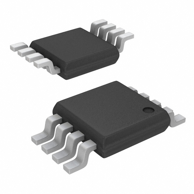
Four Buffered 8-Bit DACs in 10-Lead microSOIC
AD5314
Four Buffered 10-Bit DACs in 10-Lead microSOIC
AD5324
Four Buffered 12-Bit DACs in 10-Lead microSOICLow Power Operation: 500 A @ 3 V, 600A @ 5 V2.5 V to 5.5 V Power SupplyGuaranteed Monotonic ByDesign Over All CodesPower-Down to 80 nA @ 3 V, 200 nA @ 5 VDouble-Buffered Input LogicOutput Range: 0VREF Power-On-Reset to Zero VoltsSimultaneous Update of Outputs (LDAC Function)Low Power, SPI™, QSPI™, MICROWIRE™, andDSP-Compatible 3-Wire Serial InterfaceOn-Chip Rail-toRail Output Buffer AmplifiersTemperature Range 40 to +105ApplicationPortable Battery-Powered InstrumentsDigital Gain and Offset AdjustmentProgrammable Voltage and Current SourcesProgrammable AttenuatorsIndustrial Process ControlPinout
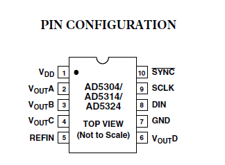
 Specifications(TA = 25°C unless otherwise noted)
VDD to GND . . . . . . . . . . . . . . . . . . . . . . . . . . 0.3 V to +7 V
Digital Input Voltage to GND . . . . . . . 0.3 V to VDD + 0.3 V
Reference Input Voltage to GND . . . . 0.3 V to VDD + 0.3 V
VOUTAD to GND . . . . . . . . . . . . . . . . 0.3 V to VDD + 0.3 V
Operating Temperature Range
Industrial (B Version) . . . . . . . . . . . . . . . 40 to +105
Storage Temperature Range . . . . . . . . . . . . 65
to +150Junction Temperature (TJ max) . . . . . . . . . . . . . . . . . . 150
10-Lead microSOIC Package
Power Dissipation . . . . . . . . . . . . . . . . . . (TJ max TA)/JA
JA Thermal Impedance . . . . . . . . . . . . . . . . . . . . 206/W
JC Thermal Impedance . . . . . . . . . . . . . . . . . . . . . 44/W
Reflow Soldering
Peak Temperature . . . . . . . . . . . . . . . . . . . . . 220 +5/0
Time at Peak Temperature . . . . . . . . . . . . 10 sec to 40 sec
| Resolution (Bits) |
12bit |
| DAC Update Rate |
125kSPS |
| DAC Settling Time |
8s |
| # DAC Outputs |
4 |
| DAC Type |
Voltage Out |
| DAC Input Format |
Ser,SPI |
| Output FSR |
(Uni Vref) |
| Ref Int/Ext |
Ext |
| Supply Vnom |
Single(+2.5),Single(+2.7),Single(+3),Single(+3.3),Single(+5) |
| Pwr Diss |
5mW |
| Package |
SOIC,SOP |
DescriptionThe AD5304/AD5314/AD5324 are quad 8-, 10- and 12-bitbuffered voltage output DACs in a 10-lead microSOIC packagethat operate from a single 2.5 V to 5.5 V supply consuming500 A at 3 V. Their on-chip output amplifiers allow rail-torailoutput swing to be achieved with a slew rate of 0.7 V/s.A 3-wire serial interface is used which operates at clock ratesup to 30 MHz and is compatible with standard SPI, QSPI,MICROWIRE and DSP interface standards.
The references for the four DACs AD5304/AD5314/AD5324 are derived from one referencepin. The outputs of all DACs may be updated simultaneouslyusing the softwareLDAC function. The parts incorporate apower-on-reset circuit that ensures that the DAC outputs powerup to zero volts and remain there until a valid write takes placeto the device. The parts contain a power-down feature thatreduces the currentconsumption of the device to 200 nA @ 5 V(80 nA @ 3 V).
The low power consumption of these parts AD5304/AD5314/AD5324 in normal operationmakes them ideally suited to portable battery-operated equipment.The power consumption is 3 mW at 5 V, 1.5 mW at 3 V, reducingto 1 W in power-down mode.
The AD5304/AD5314/AD5324* are quad 8-, 10-, and 12-bit buffered voltage output DACs in 10-lead MSOP and 10-lead LFCSP packages that operate from a single 2.5 V to 5.5 V supply, consuming
The AD5324 is designed as one kind of 2.5 V to 5.5 V, 115 uA, parallel interface single voltage-output 8-/10-/12-bit DAC that can be used in (1)portable battery-powered instruments; (2)digital gain and offset adjustment; (3)programmable voltage and current sources; (4)programmable attenuators; (5)industrial process control applications. This device incorporates an on-chip output buffer that can drive the output to both supply rails, and is also available in Thin Shrink Small Outline Packages (TSSOP).
Features of the AD5324 are:(1)low power operation: 115 uA @ 3 V, 140 uA @ 5 V; (2)power-down to 80 nA @ 3 V, 200 nA @ 5 V via PD Pin; (3)2.5 V to 5.5 V power supply; (4)double-buffered input logic; (5)guaranteed monotonic by design over all codes; (6)buffered/unbuffered reference input options; (7)output range: 0VREF or 02 VREF; (8)power-on reset to zero volts; (9)simultaneous update of DAC outputs via LDAC pin; (10)asynchronous CLR facility; (11)low power parallel data interface; (12)on-chip rail-to-rail output buffer amplifiers; (13)temperature range: 40 to +105 .
The absolute maximum ratings of the AD5324 can be summarized as:(1)VDD to GND: -0.3 V to +7 V;(2)Digital Input Voltage to GND: -0.3 V to VDD+0.3 V;(3)Digital Output Voltage to GND: -0.3 V to VDD+0.3 V;(4)Reference Input Voltage to GND: -0.3 V to VDD+0.3 V;(5)Operating Temperature Range Industrial (B Version): -40°C to +105°C;(6)Storage Temperature Range: -65°C to +150°C;(7)Junction Temperature: 150°C. If you want to know more information about it, please download the datasheet in www.seekic.com or www.chinaicmart.com .

 AD5324 Data Sheet