Series: -
Settling Time: 6µs
Number of Bits: 8
Voltage Supply Source: Single Supply
Mounting Type: Surface Mount
Operating Temperature: -40°C ~ 105°C
Packaging: Tube
Data Interface: Parallel
Number of Converters: 8
Number of Outputs and Type: 8 Voltage, Unipolar; 8 Voltage, Bipolar
Sampling Rate (Per Second): 167k
Manufacturer: Analog Devices Inc
Power Dissipation (Max): 8.3mW
Package / Case: 38-TFSOP (0.173", 4.40mm Width)
Supplier Device Package: 38-TSSOP
Features: ` AD5346: octal 8-bit DAC
` AD5347: octal 10-bit DAC
` AD5348: octal 12-bit DAC
` Low power operation: 1.4 mA (max) @ 3.6 V
` Power-down to 120 nA @ 3 V, 400 nA @ 5 V
` Guaranteed monotonic by design over all codes
` Rail-to-rail output range: 0 V to VREF or 0 V to 2 * VREF
` Power-on reset to 0 V
` Simultaneous update of DAC outputs via LDAC pin
` Asynchronous CLR facility
` Readback
` Buffered/unbuffered reference inputs
` 20 ns WR time
` 38-lead TSSOP/6 mm * 6 mm 40-lead LFCSP packaging
` Temperature range: 40°C to +105°CApplication· Portable battery-powered instruments
· Digital gain and offset adjustment
· Programmable voltage and current sources
· Optical networking
· Automatic test equipment
· Mobile communications
· Programmable attenuators
· Industrial process controlPinout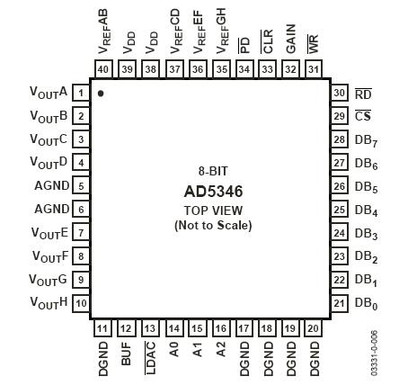 SpecificationsVDD to GND....................................................................0.3 V to +7 V
Digital Input Voltage to GND...............................0.3 V to VDD + 0.3 V
Digital Output Voltage to GND.............................0.3 V to VDD + 0.3 V
Reference Input Voltage to GND.........................0.3 V to VDD + 0.3 V
VOUT to GND.......................................................0.3 V to VDD + 0.3 V
Operating Temperature Range
Industrial (B Version).................................................40°C to +105°C
Storage Temperature Range......................................65°C to +150°C
Junction Temperature..................................................................150°C
38-Lead TSSOP Package
Power Dissipation..............................................(TJ max − TA)/ JA mW
JA Thermal Impedance.........................................................98.3°C/W
JC Thermal Impedance...........................................................8.9°C/W
40-Lead LFCSP Package
Power Dissipation ..............................................(TJ max − TA)/ JA mW
JA Thermal Impedance (3-layer board)..................................29.6°C/W
Lead Temperature, Soldering (10 sec)..........................................300°C
IR Reflow, Peak Temperature.........................................................220°CDescriptionThe AD5346/AD5347/AD53481 are octal 8-, 10-, and 12-bit DACs, operating from a 2.5 V to 5.5 V supply. These devices incorporate an on-chip output buffer that can drive the output to both supply rails, and also allow a choice of buffered or unbuffered reference input.
The AD5346/AD5347/AD5348 have a parallel interface. CS selects the device and data is loaded into the input registers on the rising edge of WR. A readback feature allows the internal DAC registers to be read back through the digital port.
The GAIN pin on these devices allows the output range to be set at 0 V to VREF or 0 V to 2 × VREF.
Input data to the DACs is double-buffered, allowing simultane-ous update of multiple DACs in a system using the LDAC pin.
An asynchronous CLR input is also provided, which resets the contents of the input register and the DAC register to all zeros. These devices also incorporate a power-on reset circuit that ensures that the DAC output powers on to 0 V and remains there until valid data is written to the device.
All three parts are pin compatible, which allows users to select the amount of resolution appropriate for their application without redesigning their circuit board.
Parameters: | Technical/Catalog Information | AD5346BRU |
| Vendor | Analog Devices Inc |
| Category | Integrated Circuits (ICs) |
| Data Interface | Parallel |
| Number of Bits | 8 |
| Operating Temperature | -40°C ~ 105°C |
| Package / Case | 38-TSSOP |
| Packaging | Tube |
| Voltage Supply Source | Single |
| Settling Time | 6s |
| Drawing Number | * |
| RoHS Status | RoHS Non-Compliant |
| Other Names | AD5346BRU
AD5346BRU
|

 AD5346BRU Data Sheet