Features: Instrumentation Amplifier Front End
Loop-Powered Operation
Precalibrated 30 mV or 60 mV Input Spans
Independently Adjustable Output Span and Zero
Precalibrated Output Spans:
420 mA Unipolar
020 mA Unipolar
12 8 mA Bipolar
Precalibrated 100 RTD Interface
6.2 V Reference with Up to 3.5 mA of Current Available
Uncommitted Auxiliary Amp for Extra Flexibility
Optional External Pass Transistor to Reduce
Self-Heating Errors
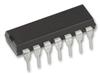
Pinout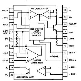 SpecificationsSupply Voltage . . . . . . . . . . . . . . . . . . . . . . . . . . . . . . . . +36 V
Reverse Loop Current . . . . . . . . . . . . . . . . . . . . . . . . . 200 mA
Signal Amp Input Range . . . . . . . . . . . . . . . . . . 0.3 V to VOP
Reference Short Circuit to Common . . . . . . . . . . . . Indefinite
Auxiliary Amp Input Voltage Range . . . . . . . . . . 0.3 V to VOP
Auxiliary Amp Current Output . . . . . . . . . . . . . . . . . . . 10 mA
Storage Temperature . . . . . . . . . . . . . . . . . . 65°C to +150°C
Lead Temperature, 10 sec Soldering . . . . . . . . . . . . . +300°C
Max Junction Temperature . . . . . . . . . . . . . . . . . . . . . +150°CDescriptionThe AD693 is a monolithic signal conditioning circuit which ccepts low-level inputs from a variety of transducers to control a tandard 420mA, two-wire current loop. An on-chip voltage eference and auxiliary amplifier are provided for transducer excitation up to 3.5mA of excitation current is available when the de is operated in the loop-powered mode. Alternatively, the device y be locally powered for three-wire applications when 020mA operation is desired. Pecalibrated 30 mV and 60 mV input spans may be set by Bmple pin strapping. Other spans from 1 mV to 100 mV may be realized with the addition of external resistors. The auxiliary aplifier may be used in combination with on-chip voltages to rovide six precalibrated ranges for 100? RTDs. Output span nd zero are also determined by pin strapping to obtain the tandard ranges: 420mA, 12 ± 8 mA and 020 mA.
Active laser trimming of the AD693's thin-film resistors result high levels of accuracy without the need for additional djustments and calibration. Total unadjusted error is tested on ery device to be less than 0.5% of full scale at +25°C, and less han 0.75% over the industrial temperature range. Residual onlinearity is under 0.05%. The AD693 also allows for the use sfan external pass transistor to further reduce errors caused by self-heating.
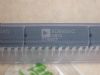
For transmission of low-level signals from RTDs, bridges and ressure transducers, the AD693 offers a cost-effective signal onditioning solution. It is recommended as a replacement for iscrete designs in a variety of applications in process control,factory automation and system monitoring. he AD693 is packaged in a 20-pin ceramic side-brazed DIP,20-pin Cerdip, and 20-pin LCCC and is specified over the -40°C to +85°C industrial temperature range.

 AD693 Data Sheet