AD7452

Features: `Specified for VDD of 3 V and 5 V`Low power at max throughput rate:3.3 mW max at 555 kSPS with 3 V supplies7.25 mW max at 555 kSPS with 5 V supplies`Fully differential analog input Wide input bandwidth:70 dB SINAD at 100 kHz input frequency`Flexible power/serial clock speed management`No...

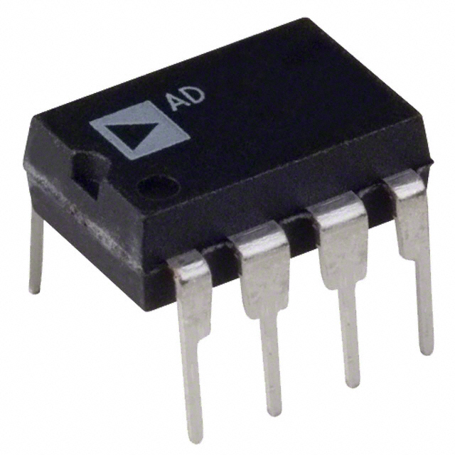
product image

AD7452 Picture
SeekIC No. : 004270210 Detail

AD7452: Features: `Specified for VDD of 3 V and 5 V`Low power at max throughput rate:3.3 mW max at 555 kSPS with 3 V supplies7.25 mW max at 555 kSPS with 5 V supplies`Fully differential analog input Wide in...

floor Price/Ceiling Price

Part Number:
AD7452
Supply Ability:
5000

Price Break

  • Qty
  • 1~5000
  • Unit Price
  • Negotiable
  • Processing time
  • 15 Days
Total Cost: $ 0.00

SeekIC Buyer Protection PLUS - newly updated for 2013!

  • Escrow Protection.
  • Guaranteed refunds.
  • Secure payments.
  • Learn more >>

Month Sales

268 Transactions

Rating

evaluate  (4.8 stars)

Upload time: 2024/4/28

Payment Methods

All payment methods are secure and covered by SeekIC Buyer Protection PLUS.

Notice: When you place an order, your payment is made to SeekIC and not to your seller. SeekIC only pays the seller after confirming you have received your order. We will also never share your payment details with your seller.
Product Details

Description


Features:

`Specified for VDD of 3 V and 5 V
`Low power at max throughput rate:
3.3 mW max at 555 kSPS with 3 V supplies
7.25 mW max at 555 kSPS with 5 V supplies
`Fully differential analog input Wide input bandwidth:
70 dB SINAD at 100 kHz input frequency
`Flexible power/serial clock speed management
`No pipeline delays
`High speed serial interface:
SPI®/QSPI™/MICROWIRE™/DSP compatible
`Power-down mode: 1 A max
`8-lead SOT-23 package


Application

·Transducer interface
·Battery-powered systems
·Data acquisition systems
·Portable instrumentation
·Motor control


Pinout

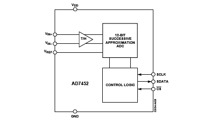
  Connection Diagram

AD7452 Diagram


Specifications

Parameter Rating
VDD to GND
VIN+ to GND
VIN to GND
Digital Input Voltage to GND
Digital Output Voltage to GND
VREF to GND
Input Current to Any Pin Except Supplies1
Operating Temperature Range
Commercial (B Version)
Storage Temperature Range
Junction Temperature
JA Thermal Impedance
JC Thermal Impedance
Lead Temperature, Soldering
Vapor Phase (60 secs)
Infrared (15 secs)
ESD
0.3 V to +7 V
0.3 V to VDD + 0.3 V
0.3 V to +7 V
0.3 V to VDD + 0.3 V
±10 mA


40 to +85
65 to +150
150
211.5/W
91.99/W

215
220
1 kV

Stresses above those listed under Absolute Maximum Ratings may cause permanent damage to the device. This is a stress rating only; functional operation of the device at these or any other conditions above those listed in the operational sections of this specification is not implied. Exposure to absolute maximum rating conditions for extended periods may affect device reliability.
1 Transient currents of up to 100 mA will not cause SCR latch-up.


Resolution (Bits) 12bit
T-Put Rate 555kSPS
# Chan 1
Supply V Single(+5),Single(+3),Single(+3.3)
Pwr Diss 7.25mW
Interface Ser,SPI
Ain Range (2Vref) p-p
SNR (dB) n/a
Pkg Type SOT


Description

The AD74521 is a 12-bit, high speed, low power, successive approximation (SAR) analog-to-digital converter that features a fully differential analog input. This part operates from a single 3 V or 5 V power supply and features throughput rates up to 555 kSPS.

The part AD7452 contains a low noise, wide bandwidth, differential track-and-hold amplifier (T/H) that can handle input frequencies up to 3.5 MHz. The reference voltage is applied externally to the VREF pin and can be varied from 100 mV to 3.5 V depending on the power supply and what suits the application. The value of the reference voltageetermines the common-mode voltage range of the part. With this truly differential input structure and variable reference input, the user can select a variety of input ranges and bias points.

The conversion process and data acquisition of AD7452 are controlled usingCS and the serial clock, allowing the device to interface with microprocessors or DSPs. The input signals are sampled on the falling edge of CS, and the conversion is also initiated at this point.

The SAR architecture of this part ensures that there are no pipeline delays.

The AD7452 uses advanced design techniques to achieve very low power dissipation


Customers Who Bought This Item Also Bought

Margin,quality,low-cost products with low minimum orders. Secure your online payments with SeekIC Buyer Protection.
Static Control, ESD, Clean Room Products
Programmers, Development Systems
Hardware, Fasteners, Accessories
Integrated Circuits (ICs)
Prototyping Products
DE1
View more