Features: Specified for VDD of 2.7 V to 5.25 V
1.75 MSPS for AD7470 (10-Bit)
1.5 MSPS for AD7472 (12-Bit)
Low Power
AD7470: 3.34 mW Typ at 1.5 MSPS with 3 V Supplies
7.97 mW Typ at 1.75 MSPS with 5 V Supplies
AD7472: 3.54 mW Typ at 1.2 MSPS with 3 V Supplies
8.7 mW Typ at 1.5 MSPS with 5 V Supplies
Wide Input Bandwidth
70 dB Typ SNR at 500 kHz Input Frequency
Flexible Power/Throughput Rate Management
No Pipeline Delays
High Speed Parallel Interface
Sleep Mode: 50 nA Typ
24-Lead SOIC and TSSOP PackagesPinout Specifications(TA = +25°C unless otherwise noted)
AVDD to AGND/DGND . . . . . . . . . . . . . . . . . 0.3 V to +7 V
DVDD to AGND/DGND . . . . . . . . . . . . . . . . . 0.3 V to +7 V
VDRIVE to AGND/DGND . . . . . . . . . . . . . . . . 0.3 V to +7 V
AVDD to DVDD . . . . . . . . . . . . . . . . . . . . . 0.3 V to +0.3 V
VDRIVE to DVDD . . . . . . . . . . . . . . 0.3 V to DVDD + 0.3 V
AGND TO DGND . . . . . . . . . . . . . . . . . . . . 0.3 V to +0.3 V
Analog Input Voltage to AGND . . . 0.3 V to AVDD + 0.3 V
Digital Input Voltage to DGND . . . .0.3 V to DVDD + 0.3 V
REF IN to AGND . . . . . . . . . . . . . . . 0.3 V to AVDD + 0.3 V
Input Current to Any Pin Except Supplies2
. . . . . . . . ±10 mA
Operating Temperature Range
Commercial (A and B Version) . . . . . . . . . 40°C to +85°C
Storage Temperature Range . . . . . . . . . 65°C to +150°C
Junction Temperature . . . . . . . . . . . . . . . . . . . . . . . +150°C
SOIC, TSSOP Package Dissipation . . . . . . . . . . . . . +450 mW
JA Thermal Impedance . . . . . . . . . . . . . . . 75°C/W (SOIC)
. . . . . . . . . . . . . . . . . . . . . . . . . . . . . . . . .115°C/W (TSSOP)
JC Thermal Impedance . . . . . . . . . . . . . . . 25°C/W (SOIC)
. . . . . . . . . . . . . . . . . . . . . . . . . . . . . . . . . 35°C/W (TSSOP)
Lead Temperature, Soldering
Vapor Phase (60 secs) . . . . . . . . . . . . . . . . . . . . . . +215°C
Infrared (15 secs) . . . . . . . . . . . . . . . . . . . . . . . . . . +220°C
| Resolution (Bits) |
10bit |
| T-Put Rate |
1.75MSPS |
| # Chan |
1 |
| Supply V |
Single(+3),Single(+3.3),Single(+5) |
| Pwr Diss |
12mW |
| Interface |
Par |
| Ain Range |
Uni (Vref) |
| SNR (dB) |
60dB |
| Pkg Type |
SOP |
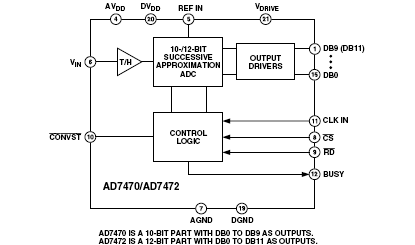
DescriptionThe AD7470/AD7472 are 10-bit/12-bit high speed, low power, successive-approximation ADCs. The parts operate from a single 2.7 V to 5.25 V power supply and feature throughput rates up to 1.5 MSPS for the 12-bit AD7472 and up to 1.75 MSPS for the 10-bit AD7470. The parts contain a low noise, wide bandwidth track/hold amplifier that can handle input frequencies in excess of 1 MHz.
The conversion process and data acquisition are controlled using standard control inputs allowing easy interfacing to microprocessors or DSPs. The input signal is sampled on the falling edge of CONVST and conversion is also initiated at this point. The BUSY goes high at the start of conversion and goes low 531.66 ns after falling edge of CONVST (AD7472 with a clock frequency of 26 MHz) to indicate that the conversion is complete. There are no pipelined delays associated with the part.
The conversion result is accessed via standard CS and RD signals over a high speed parallel interface.
The AD7470/AD7472 uses advanced design techniques to achieve very low power dissipation at high throughput rates. With 3 V supplies and 1.5 MSPS throughput rate, the AD7470 typically consumes, on average, just 1.1 mA. With 5 V supplies and 1.75 MSPS, the average current consumption is typically
1.6 mA. The part also offers flexible power/throughput rate management. Operating the AD7470 with 3 V supplies and 500 kSPS throughput reduces the current consumption to 713 A.At 5 V supplies and 500 kSPS, the part consumes 944 A.
It is also possible to operate the parts in an auto sleep mode, where the part wakes up to do a conversion and automatically enters sleep mode at the end of conversion. Using this method allows very low power dissipation numbers at lower throughput rates. In this mode, the AD7472 can be operated with 3 V supplies at 100 kSPS, and consume an average current of just 124 A.
At 5 V supplies and 100 kSPS, the average current consumption is 171 A.
The analog input range for the part is 0 to REF IN. The +2.5 V reference is applied externally to the REF IN pin. The conversion rate is determined by the externally-applied clock.

 AD7470 Data Sheet


