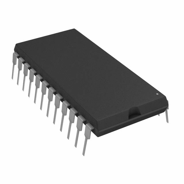
DescriptionThe AD7550BQ is one member of the AD7550 series.The AD7550 parallel output data lines have threestate logic and are microprocessor compatible through the use of two enable lines which control the lower eight LSB's (low byte enable) and the five MBS's (high byte enable). An overrange also available which together with the BUSY and flags can be interrogated through the STATUS ENABLE providing easy microprocessor interface.
Features of the AD7550BQ are:(1)microprocessor compatible; (2)ratiometric; (3)overrange flag; (4)very low power dissipation; (5)TTL/CMOS compatible; (6)CMOS monolithic construction.For most applications, the AD7550 needs only three resistors one capacitor, and a reference voltage since the integrating amplifier, comparator, switches and digital logic are all on the CMOS chip.The AD7550 uses a high density CMOS process featuring double layer metal and silicon nitride passivation to ensure high reliability and long-term stability.
The absolute maximum ratings of the AD7550BQ can be summarized as:(1)Vdd to AGND:0 to 14V;(2)storage temperature:-65 to 150;(3)operating temperature :-25 to 85;(4)power disspation:1000mW.The digital control inputs are zener protected; however,permanent damage may occur on unconnected units under high energy electrostatic fields. Keep unused units in conductive foam at all times. Prior to pulling the devices from the conductive foam, ground the foam to deplete any accumulated charge.The AD7550 conversion time is about 40ms with a 1MHz clock. Clock can be externally controlled or internally generated by simply connecting a capacitor to the clock pin.A positive start pulse can be self-generated by having a capacitor on the start pin or can be externally applied.Phase 4 integrates (VREF1-VS) and the comparator output ramps down until zero crossing once again is achieved. Since the comparator always approaches zero crossing from the same slope, propagation delay is constant and hysteresis effect is eliminated.
At present there is not too much information about this model.If you are willing to find more about AD7550BQ, please pay attention to our web! We will promptly update the relevant information.

 AD7550BQ Data Sheet