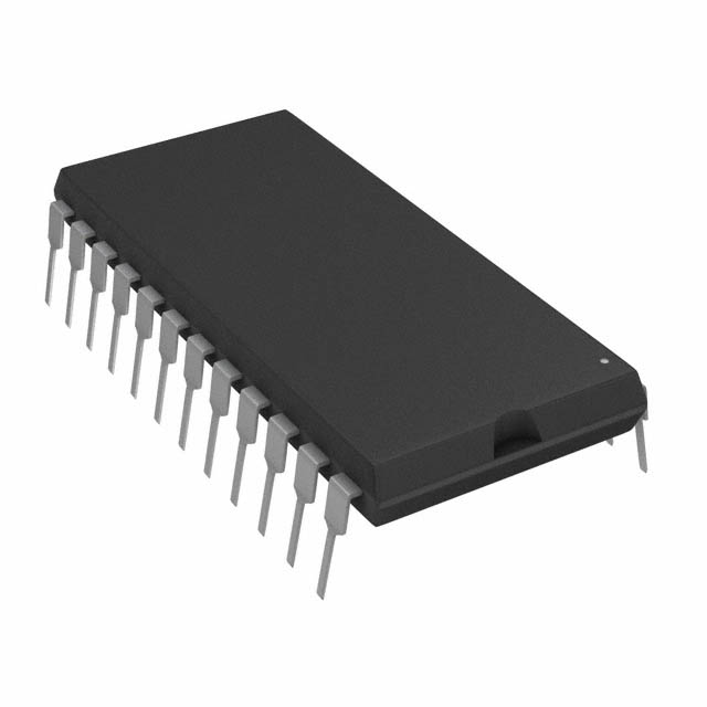
Features: SpecificationsDescription The AD7582 is designed as medium speed, 4-channel 12-bit CMOS A/D converter which uses the successive approximation technique to provide a conversion time of 100uS per channel.An auto-zero cycle occurs at the start of each conversion resulting in very low system...
AD7582: Features: SpecificationsDescription The AD7582 is designed as medium speed, 4-channel 12-bit CMOS A/D converter which uses the successive approximation technique to provide a conversion time of 100u...
SeekIC Buyer Protection PLUS - newly updated for 2013!
268 Transactions
All payment methods are secure and covered by SeekIC Buyer Protection PLUS.
The AD7582 is designed as medium speed, 4-channel 12-bit CMOS A/D converter which uses the successive approximation technique to provide a conversion time of 100uS per channel.An auto-zero cycle occurs at the start of each conversion resulting in very low system offset voltages, typically less than 100uV.
AD7582 has eight features.The first one is that it would have 12-bit successive approximation ADC.The second one is that it would have four high impredance input channels.The third one is about its analog input voltage range which means from 0 to +5V with positive reference of +5V.The fourth one is about its conversion time which would be 100uS per channel.The fifth one is that it would have no missed codes over full temperature range.The sixth one is that it would have low total unadjusted error which means +/- 1LSB max.The seventh one is that it would have autozero cycle for low offset voltage.The eighth one is that it would have monolithic constrution.That are all the features.
Some absolute maximum ratings of AD7582 have been concluded into several points as follow.The first one is about its Vdd to DGND which would be from -0.3 to +17V.The second one is about its Vss to DGND which would be from +0.3V to -7V.The third one is about its AGND to DGND which would be from -0.3V to Vref+0.3 V.The fourth one is about its Vcc to DGND which would be from -0.3 to Vdd+0.3 V.The fifth one is about its Vref to AGND which would be from -0.3 to Vdd+0.3 V.The sixth one is about its AIN (0-3) to AGND which would be from -0.3 to Vdd+0.3 V.The seventh one is about its digital input voltage to DGND which would be from -0.3 to Vdd+0.3 V.The next one is about its digital output voltage to DGND which would be from -0.3 to Vdd+0.3 V.The next one is about its operating temperature range which would be from -40 to +85°C for commercial and would be from -40 to +85°C for industrial and would be from -55 to +125°C for extended.The next one is about its storage temperature which would be from -65 to +150°C.The next one is about its junction temperature which would be +150°C.