AD7998

Features: ` 10- and 12-bit ADC with fast conversion time: 2 s typ` 8 single-ended analog input channels` Specified for VDD of 2.7 V to 5.5 V` Low power consumption` Fast throughput rate: up to 188 kSPS` Sequencer operation` Automatic cycle mode` I2C®-compatible serial interface supports standa...

product image

AD7998 Picture
SeekIC No. : 004271419 Detail

AD7998: Features: ` 10- and 12-bit ADC with fast conversion time: 2 s typ` 8 single-ended analog input channels` Specified for VDD of 2.7 V to 5.5 V` Low power consumption` Fast throughput rate: up to 188 k...

floor Price/Ceiling Price

Part Number:
AD7998
Supply Ability:
5000

Price Break

  • Qty
  • 1~5000
  • Unit Price
  • Negotiable
  • Processing time
  • 15 Days
Total Cost: $ 0.00

SeekIC Buyer Protection PLUS - newly updated for 2013!

  • Escrow Protection.
  • Guaranteed refunds.
  • Secure payments.
  • Learn more >>

Month Sales

268 Transactions

Rating

evaluate  (4.8 stars)

Upload time: 2024/4/28

Payment Methods

All payment methods are secure and covered by SeekIC Buyer Protection PLUS.

Notice: When you place an order, your payment is made to SeekIC and not to your seller. SeekIC only pays the seller after confirming you have received your order. We will also never share your payment details with your seller.
Product Details

Description


Features:

` 10- and 12-bit ADC with fast conversion time: 2 s typ
` 8 single-ended analog input channels
` Specified for VDD of 2.7 V to 5.5 V
` Low power consumption
` Fast throughput rate: up to 188 kSPS
` Sequencer operation
` Automatic cycle mode
` I2C®-compatible serial interface supports standard, fast, and high speed modes
` Out-of-range indicator/alert function
` Pin-selectable addressing via AS
` Shutdown mode: 1 A max
` Temperature range: −40°C to +85°C
` 20-lead TSSOP package
` See the AD7992 and AD7994 for 2-channel and 4-channel equivalent devices, respectively


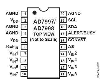
Pinout

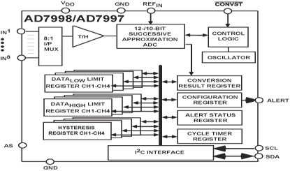
AD7998 Diagram

  Connection Diagram


Specifications

Resolution (Bits) 12bit
T-Put Rate 79kSPS
# Chan 8
Supply V Single(+3),Single(+3.3),Single(+5)
Interface I2C/Ser 2-Wire,Ser
Ain Range Uni (Vref)
SNR (dB) 71dB
Pkg Type SOP


VDD to GND........................................................−0.3 V to 7 V
Analog Input Voltage to GND...............−0.3 V to VDD + 0.3 V
Reference Input Voltage to GND..........−0.3 V to VDD + 0.3 V
Digital Input Voltage to GND...........................−0.3 V to +7 V
Digital Output Voltage to GND.............−0.3 V to VDD + 0.3 V
Input Current to Any Pin Except Supplies1...............±10 mA
Operating Temperature Range
Commercial (B Version)...............................−40°C to +85°C
Storage Temperature Range....................−65°C to +150°C
Junction Temperature................................................150°C
20-Lead TSSOP
JA Thermal Impedance.........................................143°C/W
JC Thermal Impedance...........................................45°C/W
Pb/SN Temperature, Soldering
Reflow (10 s to 30 s).....................................240 (+0/-5)°C
Pb-free Temperature, Soldering
Reflow................................................................260 (+0)°C
ESD............................................................................1.5 kV


Description

The AD7997/AD7998 are 8-channel, 10- and 12-bit, low power, successive approximation ADCs with an I2C-compatible interface. The parts operate from a single 2.7 V to 5.5 V power supply and feature a 2 s conversion time. The parts contain an 8-channel multiplexer and track-and-hold amplifier that can handle input frequencies up to 11 MHz.

The AD7997/AD7998 provide a 2-wire serial interface that is compatible with I2C interfaces. Each part comes in two versions, AD7997-0/AD7998-0 and AD7997-1/AD7998-1, and each version allows at least two different I2C addresses. The I2C interface on the AD7997-0/AD7998-0 supports standard and fast I2C interface modes. The I2C interface on the AD7997-1/ AD7998-1 supports standard, fast, and high speed I2C interface modes.

The AD7997/AD7998 normally remain in a shutdown state while not converting, and power up only for conversions. The conversion process can be controlled using the CONVST pin, by a command mode where conversions occur across I2C write operations or an automatic conversion interval mode selected through software control.

The AD7997/AD7998 require an external reference that should be applied to the REFIN pin and can be in the range of 1.2 V to VDD. This allows the widest dynamic input range to the ADC.

On-chip limit registers can be programmed with high and low limits for the conversion result, and an open-drain, out-of-range indicator output (ALERT) becomes active when the programmed high or low limits are violated by the conversion result. This output can be used as an interrupt.


Customers Who Bought This Item Also Bought

Margin,quality,low-cost products with low minimum orders. Secure your online payments with SeekIC Buyer Protection.
Resistors
Prototyping Products
DE1
Fans, Thermal Management
Memory Cards, Modules
Batteries, Chargers, Holders
View more