Features: Wide Bandwidth: 0.1 GHz to 2.5 GHz Min High Dynamic Range: 70 dB to 63.0 dB High Accuracy: ±1.0 dB over 65 dB Range (@ 1.9 GHz) Fast Response: 40 ns Full-Scale Typical Controller Mode with Error Output Scaling Stable Over Supply and Temperature Wide Supply Range: +2.7 V to +5.5 V Low Power: 40 mW at 3 V Power-Down Feature: 60 W at 3 V Complete and Easy to Use
ApplicationRF Transmitter Power Amplifier Setpoint Control and Level Monitoring Logarithmic Amplifier for RSSI Measurement Cellular Base Stations, Radio Link, Radar
Pinout Specifications
| RF Frequency (MHz) |
100 to 2500 |
| Dynamic Range (dB) |
70dB |
| Temp Stability (dB) |
±1.25dB |
| Phase Accuracy (deg) |
n/a |
| Response Time (ns typ) |
40ns |
| Voltage Supply (V) |
2.7 to 5.5 |
| Supply Current |
14mA |
| Package |
8-Lead uSOIC |
Supply Voltage VS . . . . . . . . . . . . . . . . . . . . . . . . . . . . . . .......5.5 V
VOUT, VSET, PWDN . . . . . . . . . . . . . . . . . . . . . .................. 0 V, VPOS
Input Power Differential (re: 50 W, 5.5 V) . . . . . . . . ........... +25 dBm
Input Power Single-Ended (re: 50 W, 5.5 V) . . . . . . ........... +19 dBm
Internal Power Dissipation . . . . . . . . . . . . . . . . . . . ........... . 200 mW
qJA . . . . . . . . . . . . . . . . . . . . . . . . . . . . . . . . . . . . . . ......... 200°C/W
Maximum Junction Temperature . . . . . . . . . . . . . . . . ..............+125
Operating Temperature Range . . . . . . . . . . . . ..........40 to +85
Storage Temperature Range . . . . . . . . . . . . . ..........65to +150
Lead Temperature Range (Soldering 60 sec) . . . . . . ........... . +300
*Stresses above those listed under Absolute Maximum Ratings may cause permanent damage to the device. This is a stress rating only; functional operation of the device at these or any other conditions above those indicated in the operational section of this specification is not implied. Exposure to absolute maximum rating conditions for extended periods may effect device reliability.
DescriptionThe AD8313 is an RF logarithmic detector and controller, with response extending from 0.1 to 2.5 GHz. The device is capable of accurately converting a modulated RF signal at its differential input to
The AD8313 is a complete multistage demodulating logarithmic amplifier, capable of accurately converting an RF signal at its differential input to an equivalent decibel-scaled value at its dc output. The AD8313 maintains a high degree of log conformance for signal frequencies from 0.1 GHz to 2.5 GHz and is useful over the range of 10 MHz to 3.5 GHz. The nominal input dynamic range is 65 dBm to 0 dBm (re: 50 W), and the sensitivity can be increased by 6 dB or more with a narrow band input impedance matching network or balun. Application is straightforward, requiring only a single supply of 2.7 V5.5 V and the addition of a suitable input and supply decoupling. Operating on a 3 V supply, its 13.7 mA consumption (for TA = +25) amounts to only 41 mW. A power-down feature is provided; the input is taken high to initiate a low current (20 mA) sleep mode, with a threshold at half the supply voltage.
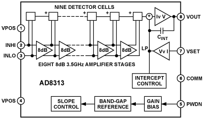
The AD8313 uses a cascade of eight amplifier/limiter cells, each having a nominal gain of 8 dB and a 3 dB bandwidth of 3.5 GHz, for a total midband gain of 64 dB. At each amplifier output, a detector (rectifier) cell is used to convert the RF signal to baseband form; a ninth detector cell is placed directly at the input of the AD8313. The current-mode outputs of these cells are summed to generate a piecewise linear approximation to the logarithmic function, and converted to a low impedance voltagemode output by a transresistance stage, which also acts as a lowpass filter.
When used as a log amp, the scaling is determined by a separate feedback interface (a transconductance stage) that sets the slope to approximately 18 mV/dB; used as a controller, this stage accepts the setpoint input. The logarithmic intercept is positioned to nearly 100 dBm, and the output runs from about 0.45 V dc at 73 dBm input to 1.75 V dc at 0 dBm input. The scale and intercept are supply and temperature stable.
The AD8313 is fabricated on Analog Devices' advanced 25 GHz silicon bipolar IC process and is available in a 8-lead mSOIC package. The operating temperature range is 40to +85. An evaluation board is available.

 AD8313 Data Sheet


