Features: Complete RF Detector/Controller Function
Typical Range 58 dBV to 13 dBV
45 dBm to 0 dBm re 50
Frequency Response from 100 MHz to 2.5 GHz
Temperature-Stable Linear-in-dB Response
Accurate to 2.5 GHz
Rapid Response: 70 ns to a 10 dB Step
Low Power: 12 mW at 2.7 V
Power-Down to 20 AApplicationCellular Handsets (TDMA, CDMA, GSM)
RSSI and TSSI for Wireless Terminal Devices
Transmitter Power Measurement and Control
Pinout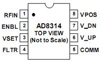
 SpecificationsSupply Voltage VPOS . . . . . . . . . . . . . . . . . . . . . .5.5 V
V_UP, V_DN, VSET, ENBL . . . . . . . . . . . . . . . 0 V, VPOS
Input Voltage . . . . . . . . . . . . . . . . . . . . . . . . 1.6 V rms
Equivalent Power . . . . . . . . . . . . . . . . . . . . . +17 dBm
Internal Power Dissipation . . . . . . . . . . . . . . 200 mW
JA . . . . . . . . . . . . . . . . . . . . . . . . . . . . . . . . .. . .200
Maximum Junction Temperature . . . . . . . . . . . . . 125
Operating Temperature Range . . . . . . 30 to +85
Storage Temperature Range . . . . . . 65 to +150
Lead Temperature Range (Soldering 60 sec) . . ..300
| RF Frequency (MHz) |
100 to 2700 |
| Dynamic Range (dB) |
45dB |
| Temp Stability (dB) |
±1dB |
| Phase Accuracy (deg) |
n/a |
| Response Time (ns typ) |
70ns |
| Voltage Supply (V) |
2.7 to 5.5 |
| Supply Current |
4.5mA |
| Package |
8-Lead uSOIC/CSP |
DescriptionThe AD8314 is a complete low-cost subsystem for the measurement and control of RF signals in the frequency range 0.1 GHz2.5 GHz, with a typical dynamic range of 45 dB, intended for use in a wide variety of cellular handsets and other wireless devices. It provides a wider dynamic range and better accuracy than possible using discrete diode detectors. In particular, its temperature stability is excellent over the full operating range of 30 to +85.
AD8314's high sensitivity allows control at low power levels, thus reducing the amount of power that needs to be coupled to the detector. It is essentially a voltage-responding device, with a typical signal range of 1.25 mV to 224 mV rms or 58 dBV to 13 dBV. This is equivalent to 45 dBm to 0 dBm re 50. For convenience, the signal is internally accoupled, using a 5 pF capacitor to a load of 3 k in shunt with 2 pF. This high-pass coupling, with a corner at 16 MHz, determines the lowest operating frequency. Thus, the source may be dc-grounded.
The AD8314 provides two voltage outputs. The first, called V_UP, increases from close to ground to about 1.2 V as the input signal level increases from 1.25 mV to 224 mV. This output is intended for use in measurement mode. Consult the Applications section of this data sheet for information on use in this mode. A capacitor may be connected between the V_UP and FLTR pins when it is desirable to increase the time interval over which averaging of the input waveform occurs.
The second output, V_DN, is an inversion of V_UP, but with twice the slope and offset by a fixed amount. This output starts at about 2.25 V (provided the supply voltage is 3.3 V) for the minimum input and falls to a value close to ground at the maximum input. This output is intended for analog control loop applications. A setpoint voltage is applied to VSET and V_DN is then used to control a VGA or power amplifier. Here again, an external filter capacitor may be added to extend the averaging time. Consult the Applications section of this data sheet for information on use in this mode.
The AD8314 is available in a micro_SOIC package and conumes 4.5 mA from a 2.7 V to 5.5 V supply. When powered down, the typical sleep current is 20 A.

 AD8314 Data Sheet