AD8362ARUZ-REEL71

Features: *Complete fully calibrated measurement/control system *Accurate rms-to-dc conversion from 50 Hz to 2.7 GHz *Input dynamic range of >60 dB: −52 dBm to +8 dBm in 50 Ω *Waveform and modulation independent: (Such as GSM/CDMA/TDMA) *Linear-in-decibels output, scaled 50 mV/dB *...

product image

AD8362ARUZ-REEL71 Picture
SeekIC No. : 004272233 Detail

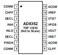
AD8362ARUZ-REEL71: Features: *Complete fully calibrated measurement/control system *Accurate rms-to-dc conversion from 50 Hz to 2.7 GHz *Input dynamic range of >60 dB: −52 dBm to +8 dBm in 50 Ω *Wavefor...

floor Price/Ceiling Price

Part Number:
AD8362ARUZ-REEL71
Supply Ability:
5000

Price Break

  • Qty
  • 1~5000
  • Unit Price
  • Negotiable
  • Processing time
  • 15 Days
Total Cost: $ 0.00

SeekIC Buyer Protection PLUS - newly updated for 2013!

  • Escrow Protection.
  • Guaranteed refunds.
  • Secure payments.
  • Learn more >>

Month Sales

268 Transactions

Rating

evaluate  (4.8 stars)

Upload time: 2024/4/23

Payment Methods

All payment methods are secure and covered by SeekIC Buyer Protection PLUS.

Notice: When you place an order, your payment is made to SeekIC and not to your seller. SeekIC only pays the seller after confirming you have received your order. We will also never share your payment details with your seller.
Product Details

Description


Features:

*Complete fully calibrated measurement/control system
*Accurate rms-to-dc conversion from 50 Hz to 2.7 GHz
*Input dynamic range of >60 dB: −52 dBm to +8 dBm in 50 Ω
*Waveform and modulation independent:
   (Such as GSM/CDMA/TDMA)
*Linear-in-decibels output, scaled 50 mV/dB
*Law conformance error of 0.5 dB
*All functions temperature and supply stable
*Operates from 4.5 V to 5.5 V at 24 mA from −40 to +85
*Power-down capability to 1.3 mW 


Application

Power amplifier linearization/control loops
Transmitter power control
Transmitter signal strength indication (TSSI)
RF instrumentation


Pinout

  Connection Diagram


Specifications

Supply Voltage VPOS................................................  5.5 V
Input Power (into Input of Device) ........................ 13 dBm
Equivalent Voltage ................................................ 2 V rms
Internal Power Dissipation..................................  500 mW
JA....................................................................... 125/W
Maximum Junction Temperature............................125/W
Operating Temperature Range ................. −40 to +85
Storage Temperature Range .................. −65 to +150
Lead Temperature Range (Soldering 60 sec) .......... 300


Description

The AD8362 is a true rms-responding power detector that has a 60 dB measurement range. It is intended for use in a variety of high frequency communication systems and in instrumentation requiring an accurate response to signal power. It is easy to use, requiring only a single supply of 5 V and a few capacitors. It can operate from arbitrarily low frequencies to over 2.7 GHz and can accept inputs that have rms values from 1 mV to at least 1 V rms, with peak crest factors of up to 6, exceeding the requirements for accurate measurement of CDMA signals.

The input signal of AD8362 is applied to a resistive ladder attenuator that comprises the input stage of a variable gain amplifier. The 12 tap points are smoothly interpolated using a proprietary technique to provide a continuously variable attenuator, which is controlled by a voltage applied to the VSET pin. The resulting signal is applied to a high performance broadband amplifier. Its output is measured by an accurate square-law detector cell. The fluctuating output is then filtered and compared with the output of an identical squarer, whose input is a fixed dc voltage applied to the VTGT pin, usually the accurate reference of 1.25 V provided at the VREF pin.

The difference in the outputs of these squaring cells AD8362 is integrated in a high gain error amplifier, generating a voltage at the VOUT pin with rail-to-rail capabilities. In a controller mode, this low noise output can be used to vary the gain of a host system's RF amplifier, thus balancing the set point against the input power. Optionally, the voltage at VSET may be a replica of the RF signal's amplitude modulation, in which case the overall effect is to remove the modulation component prior to detection and low-pass filtering. The corner frequency of the averaging filter may be lowered without limit by adding an external capacitor at the CLPF pin. The AD8362 can be used to determine the true power of a high frequency signal having a complex low frequency modulation envelope (or simply as a low frequency rms voltmeter). The high-pass corner generated by its offset-nulling loop can be lowered by a capacitor added on the CHPF pin.

Used as a power measurement device AD8362, VOUT is strapped to VSET, and the output is then proportional to the logarithm of the rms value of the input; that is, the reading is presented directly in decibels and is conveniently scaled 1 V per decade, that is, 50 mV/dB; other slopes are easily arranged. In controller modes, the voltage applied to VSET determines the power level required at the input to null the deviation from the setpoint. The output buffer can provide high load currents.

The AD8362 is powered down by a logic high applied to the PWDN pin, i.e., the consumption is reduced to about 1.3 mW. It powers up within about 20 µs to its nominal operating current of 20 mA at 25°C. The AD8362 is supplied in a 16-lead TSSOP package for operation over the industrial temperature range of −40°C to +85°C. An evaluation board is available.


Customers Who Bought This Item Also Bought

Margin,quality,low-cost products with low minimum orders. Secure your online payments with SeekIC Buyer Protection.
Power Supplies - External/Internal (Off-Board)
Optical Inspection Equipment
Transformers
Boxes, Enclosures, Racks
View more