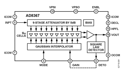
Features: Broad-range analog variable gain: −2.5 dB to +42.5 dB
3 dB cutoff frequency of 500 MHz
Gain up and gain down modes
Linear-in-dB, scaled 20 mV/dB
Resistive ground referenced input
Nominal ZIN = 200
On-chip, square-law detector
Single-supply operation: 2.7 V to 5.5 VApplicationCellular base stations
Broadband access
Power amplifier control loops
Complete, linear IF AGC amplifiers
High speed data I/OPinout
 Specifications
| Gain Control |
Analog |
| -3 dB BW (MHz) |
500MHz |
| Gain Low End (dB) |
-2.5dB |
| Gain High End (dB) |
+42.5dB |
| Number of Channels |
1 |
| Spectral Noise (nV/rtHz) |
1.84nV/rtHz |
| Supply Voltage (V) |
+5.5V |
| Supply Current |
26mA |
| Gain Accuracy (dB) |
±0.2dB |
| Parameter |
Rating |
Supply Voltage VPSO, VPSI
ENBL Voltage
MODE Select Voltage
VGAIN Control Voltage
Input Voltage
Internal Power Dissipation
JA
Maximum Junction Temperature
Operating Temperature Range
Storage Temperature Range
Lead Temperature Range (Soldering 60 sec) |
5.5 V
VS + 200 mV
VS + 200 mV
1.2 V
±600 mV
250 mW
150/W
125
−40 to +85
−65 to +150
300 |
DescriptionThe AD8367 is a high performance 45 dB variable gain amplifier with linear-in-dB gain control for use from low frequencies up to several hundred megahertz. The range, flatness, and accuracy of the gain response are achieved using Analog Devices' X-AMP® architecture, the most recent in a series of powerful proprietary concepts for variable gain applications, which far surpasses what can be achieved using competing techniques.
The input is applied to a 9-stage, 200 resistive ladder network. Each stage has 5 dB of loss, giving a total attenuation of 45 dB. At maximum gain, the first tap is selected; at progressively lower gains, the tap moves smoothly and continuously toward higher attenuation values. The attenuator is followed by a 42.5 dB fixed gain feedback amplifier-essentially an operational amplifier with a gain bandwidth product of 100 GHz-and is very linear, even at high frequencies. The output third order intercept is +20 dBV at 100 MHz (+27 dBm, re 200 ), measured at an output level of 1 V p-p with VS = 5 V. The analog gain-control input is scaled at 20 mV/dB and runs from 50 mV to 950 mV. This corresponds to a gain of −2.5 dB to +42.5 dB, respectively, when the gain up mode is selected and +42.5 dB to −2.5 dB, respectively, when gain down mode is selected. The gain down, or inverse, mode must be selected when operating in AGC in which an integrated square-law detector with an internal setpoint is used to level the output to 354 mV rms, regardless of the crest factor of the output signal. A single external capacitor sets up the loop averaging time.
The AD8367 can be powered on or off by a voltage applied to the ENBL pin. When this voltage is at a logic LO, the total power dissipation drops to the milliwatt range. For a logic HI, the chip powers up rapidly to its normal quiescent current of 26 mA at 25. The AD8367 is available in a 14-lead TSSOP package for the industrial temperature range of −40 to +85.

 AD8367 Data Sheet


