Features: Voltage feedback amplifier Ideal for ADSL and ADSL2+ central office (CO) and customer premises equipment (CPE) applications Enables high current differential applications Low power operation Single- or dual-power supply operation from 10 V (±5 V) up to 24 V (±12 V) 4 mA total quiescent s...
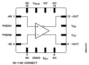
AD8390: Features: Voltage feedback amplifier Ideal for ADSL and ADSL2+ central office (CO) and customer premises equipment (CPE) applications Enables high current differential applications Low power operati...
SeekIC Buyer Protection PLUS - newly updated for 2013!
268 Transactions
All payment methods are secure and covered by SeekIC Buyer Protection PLUS.
Parameter | Rating |
Supply Voltage VOCM Package Power Dissipation Maximum Junction Temperature (T J MAX) Operating Temperature Range (TA) Storage Temperature Range Lead Temperature (Soldering 10 s) |
±13.2 V (26.4 V) VEE < VOCM < VCC (T J MAX TA)/JA 150 40 to +85 65 to +150 300 |
The AD8390 is a high output current, low power consumption differential amplifier. It is particularly well suited for the central office (CO) driver interface in digital subscriber line systems such as ADSL and ADSL2+. While in full bias operation, the driver is capable of providing 24.4 dBm output power into low resistance loads. This is enough to power a 20.4 dBm line while compensating for losses due to hybrid insertion, transformer insertion, and back termination resistors.
The AD8390 fully differential amplifier is available in a ther-mally enhanced lead frame chip scale package (LFCSP-16) and a 16-lead QSOP/EP. Significant control and flexibility in bias current have been designed into the AD8390. The four power modes are controlled by two digital bits, PWDN (1,0) which provide three levels of driver bias and one powered-down state. In addition, the IADJ pin can be used for fine quiescent current trimming to tailor the performance of the AD8390.