Features: CMOS 10-Bit 40 MSPS Sampling A/D Converter Power Dissipation: 74 mW (3 V Supply, 40 MSPS) 17 mW (3 V Supply, 5 MSPS) Operation Between 2.7 V and 3.6 V Supply Differential Nonlinearity: 60.25 LSB Power-Down (Standby) Mode, 0.65 mW ENOB: 9.55 @ fIN = 20 MHz Out-of-Range Indicator Adjustable On-Chip Voltage Reference IF Undersampling up to fIN = 130 MHz Input Range: 1 V to 2 V p-p Differential or Single-Ended Adjustable Power Consumption Internal Clamp Circuit
ApplicationCCD Imaging Video Portable Instrumentation IF and Baseband Communications Cable Modems Medical UltrasoundPinout Specifications
| Parameter |
With
Respect
to |
Min |
Max |
Units |
| AVDD |
AVSS |
0.3 |
+3.9 |
V |
| DRVDD |
DRVSS |
0.3 |
+3.9 |
V |
| AVSS |
DRVSS |
0.3 |
+0.3 |
V |
| AVDD |
DRVDD |
3.9 |
+3.9 |
V |
| REFCOM |
AVSS |
0.3 |
+0.3 |
V |
| CLK |
AVSS |
0.3 |
AVDD + 0.3 |
V |
| Digital Outputs |
DRVSS |
0.3 |
DRVDD + 0.3 |
V |
| AINP |
AINN |
AVSS 0.3 |
AVDD + 0.3 |
V |
| VREF |
AVSS |
0.3 |
AVDD + 0.3 |
V |
| REFSENSE |
AVSS |
0.3 |
AVDD + 0.3 |
V |
| REFTF, REFBF |
AVSS |
0.3 |
AVDD + 0.3 |
V |
| STBY |
AVSS |
0.3 |
AVDD + 0.3 |
V |
| CLAMP |
AVSS |
0.3 |
AVDD + 0.3 |
V |
| CLAMPIN |
AVSS |
0.3 |
AVDD + 0.3 |
V |
| PWRCON |
AVSS |
0.3 |
AVDD + 0.3 |
V |
| DFS |
AVSS |
0.3 |
AVDD + 0.3 |
V |
| 3-STATE |
AVSS |
0.3 |
AVDD + 0.3 |
V |
| Junction Temperature |
|
|
+150 |
|
| Storage Temperature |
|
65 |
+150 |
|
Lead Temperature
(10 sec) |
|
|
+300 |
|
DescriptionThe AD9203 is a monolithic low power, single supply, 10-bit, 40 MSPS analog-to-digital converter, with an on-chip voltage reference. The AD9203 uses a multistage differential pipeline architecture and guarantees no missing codes over the full operating temperature range. Its input range may be adjusted between 1 V and 2 V p-p.
The AD9203 has an onboard programmable reference. An external reference can also be chosen to suit the dc accuracy and temperature drift requirements of an application.
An external resistor can be used to reduce power consumption when operating at lower sampling rates. This yields power savings for users who do not require the maximum sample rate. This feature is especially useful at sample rates far below 40 MSPS. Excellent performance is still achieved at reduced power. For example, 9.7 ENOB performance may be realized with only 17 mW of power, using a 5 MHz clock.
A single clock input is used to control all internal conversion cycles. The digital output data is presented in straight binary or twos complementary output format by using the DFS pin. An out of-range signal (OTR) indicates an overflow condition that can be used with the most significant bit to determine over or under range.
The AD9203 can operate with a supply range from 2.7 V to 3.6 V, attractive for low power operation in high speed portable applications.
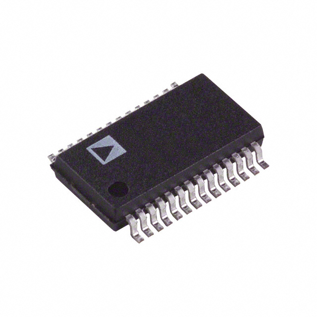
The AD9203 is specified over industrial (40 to +85) temperature ranges and is available in a 28-lead TSSOP package.

 AD9203 Data Sheet


