Series: -
Number of Converters: 1
Voltage Supply Source: Single Supply
Mounting Type: Surface Mount
Packaging: Tape & Reel (TR)Alternate Packaging
Number of Inputs and Type: 1 Single-Ended, Unipolar
Operating Temperature: -40°C ~ 85°C
Number of Bits: 8
Data Interface: Parallel
Power Dissipation (Max): 110mW
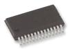
Package / Case: 28-SSOP (0.209", 5.30mm Width)
Supplier Device Package: 28-SSOP
Sampling Rate (Per Second): 32M
Manufacturer: Analog Devices Inc
DescriptionThe AD9280ARSZRL is one member of the AD9280 series.The AD9280 is a monolithic, single supply, 8-bit, 32 MSPS analog-to-digital converter with an on-chip sample-and-hold amplifier and voltage reference. The AD9280 uses a multistage differential pipeline architecture at 32 MSPS data rates and guarantees no missing codes over the full operating temperature range.The AD9280 is designed to allow optimal performance in a wide variety of imaging, communications and instrumentation applications, including pin compatibility with the AD876-8 A/D.
Features of the AD9280ARSZRL are:(1)CMOS 8-Bit 32 MSPS sampling A/D converter; (2)pin-compatible with AD876-8; (3)power dissipation: 95 mW (3 V Supply); (4)operation between +2.7 V and +5.5 V supply; (5)differential nonlinearity: 0.2 LSB; (6)power-down (sleep) mode; (7)three-state outputs; (8)out-of-range indicator; (9)built-in clamp function (DC restore); (10)adjustable on-chip voltage reference; (11)IF undersampling to 135 MHz.The input of the AD9280 has been designed to ease the development of both imaging and communications systems. The user can select a variety of input ranges and offsets and can drive the input either single-ended or differentially.
The absolute maximum ratings of the AD9280ARSZRL can be summarized as:(1)AVDD:0.3 to +6.5 V;(2)DVDD:0.3 to +6.5 V;(3)junction temperature:+150;(4)storage temperature:65 to +150;(5)lead temperature(10 sec):+300.Stresses above those listed under absolute maximum ratings may cause permanent damage to the device. This is a stress rating only; functional operation of the device at these or any other conditions above those indicated in the operational sections of this specification is not implied. Exposure to absolute maximum ratings for extended periods may effect device reliability.The first code transition should occur for an analog value 1 LSB above nominal negative full scale. The last transition should occur for an analog value 1 LSB below the nominal positive full scale. Gain error is the deviation of the actual difference between first and last code transitions and the ideal difference between the first and last code transitions.
Parameters: | Technical/Catalog Information | AD9280ARSZRL |
| Vendor | Analog Devices Inc |
| Category | Integrated Circuits (ICs) |
| Number of Bits | 8 |
| Package / Case | 28-SSOP |
| Data Interface | Parallel |
| Packaging | Tape & Reel (TR) |
| Sampling Rate (Per Second) | 32M |
| Operating Temperature | -40°C ~ 85°C |
| Voltage Supply Source | Single |
| Number of Inputs and Type | 1 Single-Ended, Unipolar |
| Number of Converters | 9 |
| Power Dissipation (Max) | 110mW |
| Drawing Number | * |
| Lead Free Status | Lead Free |
| RoHS Status | RoHS Compliant |
| Other Names | AD9280ARSZRL
AD9280ARSZRL
|
 AD9280ARSZRL Data Sheet