AD9511

Features: Low phase noise phase-locked loop coreReference input frequencies to 250 MHzProgrammable dual-modulus prescalerProgrammable charge pump (CP) currentSeparate CP supply (VCPS) extends tuning range Two 1.6 GHz, differential clock inputs 5 programmable dividers, 1 to 32, all integers Phase ...

product image

AD9511 Picture
SeekIC No. : 004273133 Detail

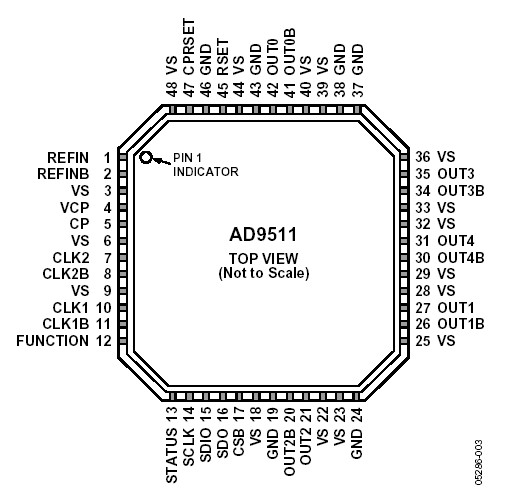
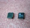
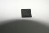
AD9511: Features: Low phase noise phase-locked loop coreReference input frequencies to 250 MHzProgrammable dual-modulus prescalerProgrammable charge pump (CP) currentSeparate CP supply (VCPS) extends tunin...

floor Price/Ceiling Price

Part Number:
AD9511
Supply Ability:
5000

Price Break

  • Qty
  • 1~5000
  • Unit Price
  • Negotiable
  • Processing time
  • 15 Days
Total Cost: $ 0.00

SeekIC Buyer Protection PLUS - newly updated for 2013!

  • Escrow Protection.
  • Guaranteed refunds.
  • Secure payments.
  • Learn more >>

Month Sales

268 Transactions

Rating

evaluate  (4.8 stars)

Upload time: 2024/4/29

Payment Methods

All payment methods are secure and covered by SeekIC Buyer Protection PLUS.

Notice: When you place an order, your payment is made to SeekIC and not to your seller. SeekIC only pays the seller after confirming you have received your order. We will also never share your payment details with your seller.
Product Details

Description


Features:

Low phase noise phase-locked loop core
Reference input frequencies to 250 MHz
Programmable dual-modulus prescaler
Programmable charge pump (CP) current
Separate CP supply (VCPS) extends tuning range
Two 1.6 GHz, differential clock inputs
5 programmable dividers, 1 to 32, all integers
Phase select for output-to-output coarse delay adjust
3 independent 1.2 GHz LVPECL outputs
Additive output jitter 225 fs rms
2 independent 800 MHz/250 MHz LVDS/CMOS clock outputs
Additive output jitter 275 fs rms
Fine delay adjust on 1 LVDS/CMOS output
Serial control port
Space-saving 48-lead LFCSP


Application

Low jitter, low phase noise clock distribution
Clocking high speed ADCs, DACs, DDSs, DDCs, DUCs, MxFEs
High performance wireless transceivers
High performance instrumentation
Broadband infrastructure


Pinout

AD9511 Diagram

  Connection Diagram


Specifications

Primary Clock Function Distribution
On-Chip Multiplier PLL Core
+Supply Voltage (V) 3.3V
Max Input Frequency 1.6GHz
# of Outputs 5
Max f-out (MHz) 1200MHz
I/O Interface Serial
Package 48-LFCSP
Output Logic CMOS,LVDS,LVPECL
Product Description Multi-Output Clock Generator


Parameter With Respect to Min Max Unit
VS
VCP
VCP
REFIN, REFINB
RSET
CPRSET
CLK1, CLK1B, CLK2, CLK2B
CLK1
CLK2
SCLK, SDIO, SDO, CSB
OUT0, OUT1, OUT2, OUT3, OUT4
FUNCTION
STATUS
Junction Temperature
Storage Temperature
Lead Temperature (10 sec)
GND
GND
VS
GND
GND
GND
GND
CLK1B
CLK2B
GND
GND


GND
GND
−0.3
−0.3
−0.3
−0.3
−0.3
−0.3
−0.3
−1.2
−1.2
−0.3
−0.3

−0.3
−0.3

−65
+3.6
+5.8
+5.8
VS + 0.3
VS + 0.3
VS + 0.3
VS + 0.3
+1.2
+1.2
VS + 0.3
VS + 0.3
VS + 0.3
VS + 0.3
150
+150
300
V
V
V
V
V
V
V
V
V
V
V

V
V
°C
°C
°C


Description

The AD9511 provides a multi-output clock distribution function along with an on-chip PLL core. The design emphasizes low jitter and phase noise to maximize data converter performance. Other applications with demanding phase noise and jitter requirements also benefit from this part.

The PLL section AD9511 consists of a programmable reference divider (R); a low noise phase frequency detector (PFD); a precision charge pump (CP); and a programmable feedback divider (N). By connecting an external VCXO or VCO to the CLK2/CLK2B pins, frequencies up to 1.6 GHz may be synchronized to the input reference.

AD9511 have five independent clock outputs. Three outputs are LVPECL (1.2 GHz), and two are selectable as either LVDS (800 MHz) or CMOS (250 MHz) levels.

Each output has a programmable divider that may be bypassed or set to divide by any integer up to 32. The phase of one clock output relative to another clock output may be varied by means of a divider phase select function that serves as a coarse timing adjustment. One of the LVDS/CMOS outputs features a programmable delay element with full-scale ranges up to 10 ns of delay. This fine tuning delay block has 5-bit resolution, giving 32 possible delays from which to choose for each full-scale setting.

The AD9511 is ideally suited for data converter clocking applications where maximum converter performance is achieved by encode signals with subpicosecond jitter.

The AD9511 is available in a 48-lead LFCSP and can be operated from a single 3.3 V supply. An external VCO, which requires an extended voltage range, can be accommodated by connecting the charge pump supply (VCP) to 5.5 V. The temperature range is −40°C to +85°C.


Customers Who Bought This Item Also Bought

Margin,quality,low-cost products with low minimum orders. Secure your online payments with SeekIC Buyer Protection.
Programmers, Development Systems
Optical Inspection Equipment
Motors, Solenoids, Driver Boards/Modules
Potentiometers, Variable Resistors
Cable Assemblies
Memory Cards, Modules
View more