Features: High-Performance Member of Pin-Compatible
TxDAC Product Family
Excellent Spurious-Free Dynamic Range Performance
SNR @ 5 MHz Output, 125 MSPS: 65 dB
Two's Complement or Straight Binary Data Format
Differential Current Outputs: 2 mA to 20 mA
Power Dissipation: 135 mW @ 3.3 V
Power-Down Mode: 15 mW @ 3.3 V
On-Chip 1.20 V Reference
CMOS-Compatible Digital Interface
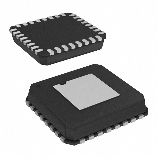
Package: 28-Lead SOIC and TSSOP Packages
Edge-Triggered LatchesApplicationWideband Communication Transmit Channel:
Direct IF
Base Stations
Wireless Local Loop
Digital Radio Link
Direct Digital Synthesis (DDS)
InstrumentationPinout Specifications
| Resolution (Bits) |
10bit |
| DAC Update Rate |
210MSPS |
| DAC Settling Time |
11ns |
| # DAC Outputs |
1 |
| DAC Type |
Current Out |
| DAC Input Format |
Par |
| Output FSR |
(Iout x Rload),Adj(Uni 2mA to Uni 20mA),User Def. Range/Offset |
| Ref Int/Ext |
Int/Ext |
| Supply Vnom |
Single(+3.3) |
| Pwr Diss (Max) |
145mW |
| Package |
CSP,SOIC,SOP |
DescriptionThe AD9740 is a 10-bit resolution, wideband, third generation member of the TxDAC series of high-performance, low power CMOS digital-to-analog converters (DACs). The TxDAC family, consisting of pin-compatible 8-, 10-, 12-, and 14-bit DACs, is specifically optimized for the transmit signal path of communication systems. All of the devices share the same interface options, small outline package, and pinout, providing an upward or downward component selection path based on performance, resolution, and cost. The AD9740 offers exceptional ac and dc performance while supporting update rates up to 165 MSPS.
The AD9740's low power dissipation makes it well suited for portable and low power applications. Its power dissipation can be further reduced to a mere 60 mW with a slight degradation in performance by lowering the full-scale current output. Also, a power-down mode reduces the standby power dissipation to approximately 15 mW. A segmented current source architecture is combined with a proprietary switching technique to reduce spurious components and enhance dynamic performance. Edge- triggered input latches and a 1.2 V temperature compensated
band gap reference have been integrated to provide a complete monolithic DAC solution. The digital inputs support 3 V CMOS logic families.

 AD9740 Data Sheet