Features: 10-Bit Dual Muxed Port DAC300 MSPS Output Update RateExcellent SFDR and IMD PerformanceSFDR to Nyquist @ 25 MHz Output: 64 dBInternal Clock Doubling PLLDifferential or Single-Ended Clock InputOn-Chip 1.2 V ReferenceSingle 3.3 V Supply OperationPower Dissipation: 155 mW @ 3.3 V48-Lead LQF...
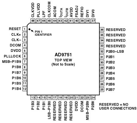
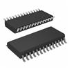
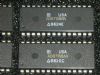
AD9751: Features: 10-Bit Dual Muxed Port DAC300 MSPS Output Update RateExcellent SFDR and IMD PerformanceSFDR to Nyquist @ 25 MHz Output: 64 dBInternal Clock Doubling PLLDifferential or Single-Ended Clock I...
SeekIC Buyer Protection PLUS - newly updated for 2013!
268 Transactions
All payment methods are secure and covered by SeekIC Buyer Protection PLUS.
Parameter | With Respect to | Min | Max | Unit |
AVDD, DVDD, CLKVDD, PLLVDD AVDD, DVDD, CLKVDD, PLLVDD ACOM, DCOM, CLKCOM, PLLCOM REFIO, REFLO, FSADJ IOUTA, IOUTB Digital Data Inputs (DB9 to DB0) CLK+/CLK, PLLLOCK DIV0, DIV1, RESET LPF Junction Temperature Storage Temperature Lead Temperature (10 sec) |
ACOM, DCOM, CLKCOM, PLLCOM ACOM, DCOM, CLKCOM, PLLCOM ACOM, DCOM, CLKCOM, PLLCOM ACOM ACOM DCOM CLKCOM CLKCOM PLLCOM |
0.3 65 |
+3.9 +3.9 +3.9 AVDD + 0.3 AVDD + 0.3 DVDD + 0.3 CLKVDD + 0.3 CLKVDD + 0.3 PLLVDD + 0.3 150 +150 300 |
V V V V V V V V V °C °C °C |
Resolution (Bits) | 10bit |
DAC Update Rate | 300MSPS |
DAC Settling Time | 11ns |
# DAC Outputs | 1 |
DAC Type | Current Out |
DAC Input Format | Par |
Output FSR | (Iout x Rload),Adj(Uni 2mA to Uni 20mA),User Def. Range/Offset |
Ref Int/Ext | Int/Ext |
Supply Vnom | Single(+3.3) |
Pwr Diss (Max) | 165mW |
Package | QFP |
The AD9751 is a dual muxed port, ultrahigh-speed, single-channel, 10-bit CMOS DAC. It integrates a high-quality 10-bit TxDAC+core, a voltage reference, and digital interface circuitry into a small 48-lead LQFP package. The AD9751 offers excep-tional ac and dc performance while supporting update rates up to 300 MSPS.
The AD9751 has been optimized for ultrahigh-speed applica-tions up to 300 MSPS where data rates exceed those possible on a single data interface port DAC. The digital interface consists
of two buffered latches as well as control logic. These latches can be time multiplexed to the high-speed DAC in several ways. This PLL drives the DAC latch at twice the speed of the exter-
nally applied clock and is able to interleave the data from the two input channels. The resulting output data rate is twice that of the two input channels. With the PLL disabled, an external
2* clock may be supplied and divided by two internally.The CLK inputs (CLK+/CLK) can be driven either differen-tially or single-endedly, with a signal swing as low as 1 V p-p.
The DAC AD9751 utilizes a segmented current source architecture com-bined with a proprietary switching technique to reduce glitch energy and to maximize dynamic accuracy. Differential current
outputs support single-ended or differential applications. The differential outputs each provide a nominal full-scale current from 2 mA to 20 mA.
The AD9751 is manufactured on an advanced low cost 0.35m CMOS process. It operates from a single supply of 3.1 V to 3.5V and consumes 155 mW of power.