Features: 12-Bit Dual Transmit DAC
125 MSPS Update Rate
Excellent SFDR to Nyquist @ 5 MHz Output: 75 dBc
Excellent Gain and Offset Matching: 0.1%
Fully Independent or Single Resistor Gain Control
Dual Port or Interleaved Data
On-Chip 1.2 V Reference
Single 5 V or 3 V Supply Operation
Power Dissipation: 380 mW @ 5 V
Power-Down Mode: 50 mW @ 5 V
48-Lead LQFPApplicationCommunications
Base Stations
Digital Synthesis
Quadrature ModulationPinout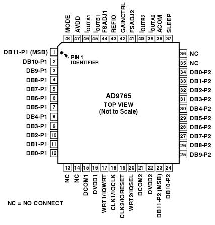 Specifications
| Parameter |
With Respectto |
Min |
Max |
Unit |
AVDD
DVDD
ACOM
AVDD
MODE, CLK1, CLK2, WRT1, WRT2
Digital Inputs
IOUTA1/IOUTA2, IOUTB1/IOUTB2
REFIO, FSADJ1, FSADJ2
GAINCTRL, SLEEP
Junction Temperature
Storage Temperature
Lead Temperature (10 sec) |
ACOM
DCOM
DCOM
DVDD
DCOM
DCOM
ACOM
ACOM
ACOM |
0.3
0.3
0.3
6.5
0.3
0.3
1.0
0.3
0.3
65 |
+6.5
+6.5
+0.3
+6.5
DVDD + 0
DVDD + 0
AVDD + 0
AVDD + 0
AVDD + 0
+150
+150
+300 |
V
V
V
V
V
V
V
V
V
°C
°C
°C |
DescriptionThe AD9765 is a dual port, high speed, two channel, 12-bit CMOS DAC. It integrates two high quality 12-bit TxDAC+cores, a voltage reference and digital interface circuitry into a small 48-lead LQFP package. The AD9765 offers exceptional ac and dc performance while supporting update rates up to 125 MSPS.
The AD9765 has been optimized for processing I and Q data in communications applications. The digital interface consists of two double-buffered latches as well as control logic. Separate
write inputs allow data to be written to the two DAC ports independent of one another. Separate clocks control the update rate of the DACs.
A mode control pin allows the AD9765 to interface to two separate data ports, or to a single interleaved high speed data port. In inter-leaving mode the input data stream is demuxed into its original I and Q data and then latched. The I and Q data is then con-verted by the two DACs and updated at half the input data rate.
The GAINCTRL pin allows two modes for setting the full-scale current (IOUTFS) of the two DACs. IOUTFS for each DAC can be set independently using two external resistors, or IOUTFS for both2 DACs can be set by using a single external resistor. The DACs utilize a segmented current source architecture com-bined with a proprietary switching technique to reduce glitch
energy and to maximize dynamic accuracy. Each DAC provides differential current output thus supporting single-ended or dif-ferential applications. Both DACs can be simultaneously updated
TxDAC+ is a registered trademark of Analog Devices, Inc.
1Patent pending.
2Please see GAINCTRL Mode section, for important date code information on
this feature.

 AD9765 Data Sheet