Features: 5 ns Settling Time
100 MSPS Update Rate
20 mA Output Current
ECL-Compatible
40 MHz Multiplying Mode
ApplicationRaster Scan & Vector Graphic Displays
High Speed Waveform Generation
Digital VCOs
Ultrafast Digital Attenuators
Pinout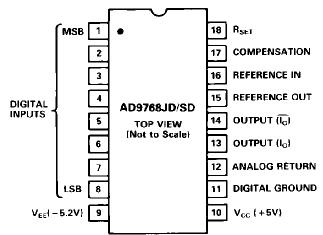 Specifications
| Parameter |
Unit |
AD9768SJD/SD/SE |
| RESOLUTION(FS = FULL SCALE) |
Bits |
8 |
| LSB WEIGHT (CURRENT) |
A |
78 |
ACCURACY1
Differential Nonlinearity
Integral Nonlinearity
Monotonicity
Zero Offset (lnitial) |
± % FS
± % FS
A |
0.2
0.2
Guaranteed
60 |
TEMPERATURE COEFFICIENTS
Zero Offset
Reference Voltage (1.26 V) |
ppm/°C
ppm/°C |
1.5
70 |
DIGITAL DATA INPUTS
Logic Compatibility
Logic Voltage Levels "l" =
"0" =
Coding |
V
V
Binary (BIN) = Unipolar
Offset Binary (OBN) = Bipolar |
ECL
0.9
1.7
Out
Out |
OUTPUT
Current (Unipolar) FS
IOUT (@ Pin 13)
All Digital "1" Input
All Digital "0" Input
IOUT(@ Pin 14)
All Digital "l" Input
All Digital "0" Input
Compliance
Impedance |
mA (max)
mA
mA
mA
mA
V (Pin 13)
V (Pin 14)
(±15%) |
2 to 20 (30)
20
0
0
20
0.7 to +3.0
1.1 to +3.0
750 |
SPEED PERFORMANCE
Settling Time (to 0.2% FS)2
Slew Rate
Update Rate
Rise Time
Glitch Energy |
ns
V/s
MSPS
ns
pV-sec |
5
400
100
1.8
200 |
REFERENCE
Internal, Monolithic3
External, Variable4
Voltage-Multiplying Mode
Current-Multiplying Mode |
V
V (max)
mA (max) |
1.26
0 to 1.1 (2)
0 to 5 (7.5 ) |
VOLTAGE-MULTIPLYING MODE4 (See Figure 2)
VM Range (at Pin 16)
VM Center
Resistance (at Pin 16)
Transfer Function
Large Signal Bandwidth (3 dB Point) |
V
V
k 800
Measured at Pin 13; Digital "0" Applied
to Bits 1-8:
0.1 VM Input = 0 mA IOUT
1.1 VM Input = 0 mA IOUT
Measured at Pin 13; Digital "1" Applied
to Bits 1-8:
0.1 VM Input = 1 mA IOUT
1.1 VM Input = 20 mA IOUT
kHz |
±0.5
0.6
800
250 |
DescriptionThe Analog Devices AD9768SD D/A converter is a monolithic current-output converter which can accept 8 bits of ECL-level digital input voltages and convert them into analog signals at
update rates as high as 100 MSPS. In addition to its use as a standard D/A converter, it can also be utilized as a two-quadrant multiplying D/A at multiplying bandwidths as high as 40 MHz.
An inherently low glitch design is used, and the complementar current outputs are suitable for driving transmission lines directly. Nominal full-scale output is 20 mA, which correspond to a 1 volt drop across a 50 load, or ±1 volt across 100 returned to +1 volt. The actual output current is determined b the on-chip reference voltage (VREF 1.26 V) and an externa current setting resistor, RSET.Full-scale output current IOUT with digital "1" at all inputs is calculated with the equation:
The setting resistor RSET and the output load resistor should both have low temperature coefficients. A complementary IOUT is also provided.
The reference voltage source is a modified bandgap type and is nominally 1.26 volts. This reference supply requires no external regulation. To reduce the possibility of noise generation and/or instability, Pin 15 (REFERENCE OUT) can be decoupled using a high-quality ceramic chip capacitor. Stabilization of the internal loop amplifier is by a single capacitor connected from Pin 17 (COMPENSATION) to ground. The minimum value for this capacitor is 3900 pF,although a 0.01 F ceramic chip capacitor is recommended.The incredible speed characteristics of the AD9768SD D/A converter make it attractive for a wide range of high speed applications. The ability of the unit to operate as a two-quadrant multiplying D/A converter adds another dimen-
sion to its usefulness and makes the AD9768SD a truly versatile device.

 AD9768 Data Sheet