AD9866

Features: Low cost 3.3 V CMOS MxFETM for broadband modems 12-bit D/A converter2×/4× interpolation filter200 MSPS DAC update rateIntegrated 23 dBm line driver with 19.5 dB gain control12-bit, 80 MSPS A/D converter−12 dB to +48 dB low noise RxPGA (< 2.5 nV/rtHz)Third order programmable low-...

product image

AD9866 Picture
SeekIC No. : 004273609 Detail

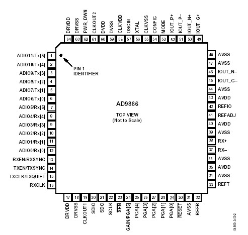
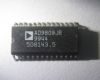
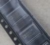
AD9866: Features: Low cost 3.3 V CMOS MxFETM for broadband modems 12-bit D/A converter2×/4× interpolation filter200 MSPS DAC update rateIntegrated 23 dBm line driver with 19.5 dB gain control12-bit, 80 MSPS...

floor Price/Ceiling Price

Part Number:
AD9866
Supply Ability:
5000

Price Break

  • Qty
  • 1~5000
  • Unit Price
  • Negotiable
  • Processing time
  • 15 Days
Total Cost: $ 0.00

SeekIC Buyer Protection PLUS - newly updated for 2013!

  • Escrow Protection.
  • Guaranteed refunds.
  • Secure payments.
  • Learn more >>

Month Sales

268 Transactions

Rating

evaluate  (4.8 stars)

Upload time: 2024/4/26

Payment Methods

All payment methods are secure and covered by SeekIC Buyer Protection PLUS.

Notice: When you place an order, your payment is made to SeekIC and not to your seller. SeekIC only pays the seller after confirming you have received your order. We will also never share your payment details with your seller.
Product Details

Description


Features:

Low cost 3.3 V CMOS MxFETM for broadband modems 12-bit D/A converter
2×/4× interpolation filter
200 MSPS DAC update rate
Integrated 23 dBm line driver with 19.5 dB gain control
12-bit, 80 MSPS A/D converter
−12 dB to +48 dB low noise RxPGA (< 2.5 nV/rtHz)
Third order programmable low-pass filter
Flexible digital data path interface
Half- and full-duplex operation
Backward compatible with AD9975 and AD9876
Various power-down/reduction modes
Internal clock multiplier (PLL)
2 auxiliary programmable clock outputs
Available in 64-lead chip scale package or bare die


Application

·Powerline networking
·VDSL and HPNA


Pinout

  Connection Diagram


Specifications

Resolution (Bits) 12bit
T-Put Rate 80MSPS
# Chan 1
Supply V Single(+3.3)
Sample Rate 80MSPS
ADC Bits x #ADCs-Speed 12x1-80 MHz
DAC Bits x #DACs-ClkSpeed 12x1-200 MHz
Pkg Type CSP
Primary Application Broadband Wireline, Home Networking


Description

The AD9866 is a mixed-signal front end (MxFE?) IC for transceiver applications requiring Tx and Rx path functionality with data rates up to 80 MSPS. Its flexible digital interface, power saving modes,

The AD9866 is a mixed-signal front end (MxFE) IC for transceiver applications requiring Tx and Rx path functionality with data rates up to 80 MSPS. Its flexible digital interface, power saving modes, and high Tx-to-Rx isolation make it well suited for half- and full-duplex applications. The digital inter-face is extremely flexible allowing simple interfaces to digital back ends that support half- or full-duplex data transfers, thus often allowing the AD9866 to replace discrete ADC and DAC solutions. Power saving modes include the ability to reduce power consumption of individual functional blocks or to power down unused blocks in half-duplex applications. A serial port interface (SPI®) allows software programming of the various functional blocks. An on-chip PLL clock multiplier and synthesizer provide all the required internal clocks, as well as two external clocks from a single crystal or clock source.

The AD9866 Tx signal path consists of a bypassable 2*/4* low-pass interpolation filter, a 12-bit TxDAC, and a line driver. The transmit path signal bandwidth can be as high as 34 MHz at an input data rate of 80 MSPS. The TxDAC provides differential current outputs that can be steered directly to an external loador to an internal low distortion current amplifier. The current amplifier (IAMP) can be configured as a current or voltage mode line driver (with two external npn transistors) capable of delivering in excess of 23 dBm peak signal power. Tx power can be digitally controlled over a 19.5 dB range in 0.5 dB steps.

The AD9866 receive path consists of a programmable amplifier (RxPGA), a tunable low pass filter (LPF), and a 12-bit ADC. The low noise RxPGA has a programmable gain range of -12 dB to +48 dB in 1 dB steps. Its input referred noise is less than 3.3 nV/rtHz for gain settings beyond 30 dB. The receive path LPF cutoff frequency can either be set over a 15 MHz to 35 MHz range or simply bypassed. The 12-bit ADC achieves excellent dynamic performance over a 5 MSPS to 80 MSPS span. Both the RxPGA and the ADC offer scalable power consumption allowing power/performance optimization.

The AD9866 provides a highly integrated solution for many broadband modems. It is available in a space-saving 64-lead chip scale package and is specified over the commercial (-40 to +85) temperature range.


Customers Who Bought This Item Also Bought

Margin,quality,low-cost products with low minimum orders. Secure your online payments with SeekIC Buyer Protection.
Memory Cards, Modules
Motors, Solenoids, Driver Boards/Modules
Crystals and Oscillators
Isolators
Fans, Thermal Management
View more