ADC083000

Features: · Internal Sample-and-Hold· Single +1.9V ±0.1V Operation· Choice of SDR or DDR output clocking· 1:2 or 1:4 Selectable Output Demux· Clock Phase Adjust for Multiple ADC Synchronization· Guaranteed No Missing Codes· Serial Interface for Extended Control· Adjustment of Input Full-Scale Rang...

product image

ADC083000 Picture
SeekIC No. : 004273987 Detail

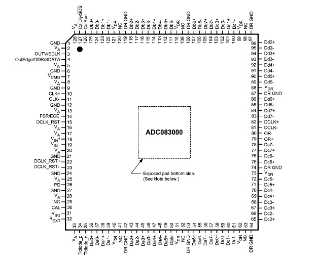
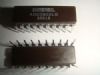
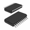
ADC083000: Features: · Internal Sample-and-Hold· Single +1.9V ±0.1V Operation· Choice of SDR or DDR output clocking· 1:2 or 1:4 Selectable Output Demux· Clock Phase Adjust for Multiple ADC Synchronization· Gua...

floor Price/Ceiling Price

Part Number:
ADC083000
Supply Ability:
5000

Price Break

  • Qty
  • 1~5000
  • Unit Price
  • Negotiable
  • Processing time
  • 15 Days
Total Cost: $ 0.00

SeekIC Buyer Protection PLUS - newly updated for 2013!

  • Escrow Protection.
  • Guaranteed refunds.
  • Secure payments.
  • Learn more >>

Month Sales

268 Transactions

Rating

evaluate  (4.8 stars)

Upload time: 2024/4/28

Payment Methods

All payment methods are secure and covered by SeekIC Buyer Protection PLUS.

Notice: When you place an order, your payment is made to SeekIC and not to your seller. SeekIC only pays the seller after confirming you have received your order. We will also never share your payment details with your seller.
Product Details

Description


Features:

· Internal Sample-and-Hold
· Single +1.9V ±0.1V Operation
· Choice of SDR or DDR output clocking
· 1:2 or 1:4 Selectable Output Demux
· Clock Phase Adjust for Multiple ADC Synchronization
· Guaranteed No Missing Codes
· Serial Interface for Extended Control
· Adjustment of Input Full-Scale Range and Offset
· Duty Cycle Corrected Sample Clock
· Test pattern


Application

· Direct RF Down Conversion
· Digital Oscilloscopes
· Satellite Set-top boxes
· Communications Systems
· Test Instrumentation


Pinout

  Connection Diagram


Specifications

(Notes 1, 2)
If Military/Aerospace specified devices are required, please contact the National Semiconductor Sales Office/ Distributors for availability and specifications.
Supply Voltage (VA, VDR).................... 2.2V
Voltage on Any Input Pin........... −0.15V to (VA +0.15V)
Ground Difference
|GND - DR GND|.................... 0V to 100 mV
Input Current at Any Pin (Note 3)............. ±25 mA
Package Input Current (Note 3) ..............±50 mA
Power Dissipation at TA 85°C.............. TBD W
ESD Susceptibility (Note 4)
Human Body Mode......................l2500V

Machine Model.........................250V

Storage Temperature ..............−65°C to +150°C
Soldering process must comply with National Semiconductor's Reflow Temperature Profile specifications. Refer to www.national.com/packaging. (Note 5)


Resolution 8 bits
Channels 1 Channels
SNR 45.3 dB
SFDR 57 dB
ENOB 7.2 bits
Max Sample Rate 3000 MSPS
Min Sample Rate 1000 MSPS
Power Dissipation 1.9 Watt
PowerWise Rating 1 4.31 pJ/conv
DNL (+/-) 0.2 LSB
INL (+/-) 0.35 LSB
SINAD 45 dB
THD dB -57 dB
Min Supply Voltage 1.8 Volt
Max Supply Voltage 2 Volt
Nominal Vin 0.7 Vpp
Temperature Min -40 deg C
Temperature Max 85 deg C
Data Converter Type ADC
Automotive Selection Guide Yes
PowerWise Yes
View Using Catalog


Description

Note: This product is currently in development. - ALL specifications are design targets and are subject to change .

The ADC083000 is a single, low power, high performance CMOS analog-to-digital converter that digitizes signals to 8 bits resolution at sampling rates up to 3.4 GSPS. Consuming a typical 1.8 Watts at 3 GSPS from a single 1.9 Volt supply, this device is guaranteed to have no missing codes over the full operating temperature range. The unique folding and interpolating architecture, the fully differential comparator design, the innovative design of the internal sample-and-hold amplifier and the self-calibration scheme enable a very flat response of all dynamic parameters up to Nyquist, producing a high 7.0 Effective Number Of Bits, (ENOB) with a 748 MHz input signal and a 3 GHz sample rate while providing a 10-18 Bit Error Rate, (BER). The ADC083000 achieves a 3 GSPS sampling rate by utilizing both the rising and falling edge of a 1.5 GHz input clock. Output formatting is offset binary and the LVDS digital outputs are compliant with IEEE 1596.3-1996, with the exception of an adjustable common mode voltage between 0.8V and 1.2V.

The ADC083000 ADC has a 1:4 demultiplexer that feeds four LVDS buses and reduces the output data rate on each bus to a quarter of the sampling rate. The ADC can be programmed into the 1:2 Output Mode where the data is output on the Dc and Dd channels at the rate of the input clock.

The ADC083000 converter typically consumes less than 20 mW in the Power Down Mode and is available in a 128-lead, thermally enhanced exposed pad LQFP and operates over the Industrial (-40°C TA +85°C) temperature range.


Customers Who Bought This Item Also Bought

Margin,quality,low-cost products with low minimum orders. Secure your online payments with SeekIC Buyer Protection.
Semiconductor Modules
Memory Cards, Modules
Connectors, Interconnects
Cables, Wires
Programmers, Development Systems
View more