Features: Bidirectional Level Translation
Operates from 1.2 V to 5.5 V
ApplicationSPITM, MicrowireTM and I2CTM Translation
Low Voltage ASIC level Translation
Smart Card Readers
Cell Phones & Cell-Phone Cradles
Portable Communication Devices
Telecommunicatons Equipment
Network Switches and Routers
Storage Systems (SAN/NAS)
Computing/Server Applications
GPS
Portable POS Systems
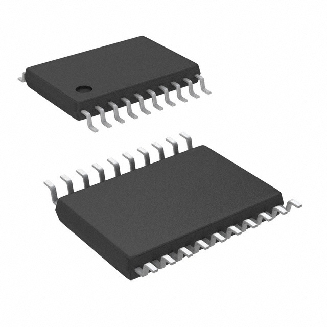
Low Cost Serial InterfacesPinout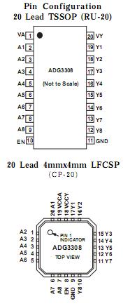
 SpecificationsVCCY to GND . . . . . . . . . . . . . . . . . . . . . . . . .-0.3 V to +7 V
VCCA to GND . . . . . . . . . . . . . . . . . . . . . . . . . -0.3 V to +7 V
Digtal Inputs (A) . . . . . . . . . . . .. -0.3 V to (VCCA +0.3V)
Digtal Inputs (Y) . . . . . . . . . . . . . . -0.3 V to (VCCY +0.3V)
EN to GND . . . . . . . . . . . . . . . . . . . . . . . . . -0.3 V to +7 V
Operating Temperature Range
Industrial (B Version) . . . . . . . . . . . . . . 40°C to +85°C
Storage Temperature Range . . . . . . . . . 65°C to +150°C
Junction Temperature . . . . . . . . . . . . . . . . . . . . . . . . 150°C
20 Lead TSSOP
JA Thermal Impedance . . . . . . . . . . . . . . . . .. . . 143°C/W
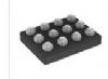
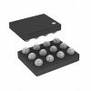
20 Lead LFCSP - 4 layer board
JA Thermal Impedance . . . . . . . . . . . . . . . . . . . . . 32°C/W
Lead Temperature, Soldering (10seconds) . . . . . . . 300°C
IR Reflow, Peak Temperature (<20 seconds) . . . +235°C
| Data Rate (typ) |
60Mbps |
| t Prop Delay (typ) |
5ns |
| Bus Enable Time (typ) |
1s |
| VCC 1 (V) |
1.15 - 5.5 |
| ICC2 |
1A |
| Pkg |
CSP,TSSOP |
| Temp Range (°C) |
-40 to 85 |
| Vcc 2 (V) |
1.65V - 5.5V |
| Bus Width |
8 |
DescriptionThe ADG3308 is an 8-Channel bidirectional level translator. Its function is to provide level shifting in a multivoltage system. The voltage applied to V
CCA sets up the logic levels on the A side of the device, while V
CCY sets the levels on the Y side. In this way, signals applied to the V
CCA side of the device appear as V
CCY compatible logic on the other side of the device and vice versa as ADG3308 is designed to handle bidirectional signals. The device is guaranteed for operation over the supply range 1.2 V to 5.5 V.
ADG3308 is suited to applications like data transfer between a low voltage DSP/Controller and a higher voltage device. Other applications include high end consumer products where constant changes to the chipset desgins result in multiple supply levels in the application. V
CCY operates from +1.65 to 5.5 V while V
CCA from +1.2 to V
CCY. V
CCA must always operate from a supply that is lower than V
CCY. When the device Enable pin (EN) is pulled low, the Ax and Yx inputs/outputs are tri-stated. The EN pin is driven high for normal operation. EN pin is referred to VCCY voltage.

 ADG3308 Data Sheet