ADG439F*

Features: Fast Switching Times tON 250 ns max tOFF 150 ns maxFault and Overvoltage Protection (40 V, +55 V)All Switches OFF with Power Supply OFFAnalog Output of ON Channel Clamped Within Power Supplies If an Overvoltage OccursLatch-Up Proof ConstructionBreak Before Make ConstructionTTL and CMOS C...

product image

ADG439F* Picture
SeekIC No. : 004274962 Detail

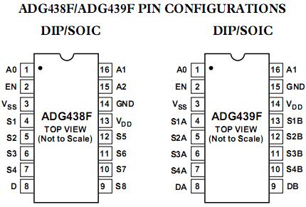
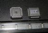
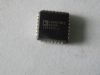
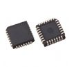
ADG439F*: Features: Fast Switching Times tON 250 ns max tOFF 150 ns maxFault and Overvoltage Protection (40 V, +55 V)All Switches OFF with Power Supply OFFAnalog Output of ON Channel Clamped Within Power Supp...

floor Price/Ceiling Price

Part Number:
ADG439F*
Supply Ability:
5000

Price Break

  • Qty
  • 1~5000
  • Unit Price
  • Negotiable
  • Processing time
  • 15 Days
Total Cost: $ 0.00

SeekIC Buyer Protection PLUS - newly updated for 2013!

  • Escrow Protection.
  • Guaranteed refunds.
  • Secure payments.
  • Learn more >>

Month Sales

268 Transactions

Rating

evaluate  (4.8 stars)

Upload time: 2024/5/2

Payment Methods

All payment methods are secure and covered by SeekIC Buyer Protection PLUS.

Notice: When you place an order, your payment is made to SeekIC and not to your seller. SeekIC only pays the seller after confirming you have received your order. We will also never share your payment details with your seller.
Product Details

Description


Features:

Fast Switching Times
  tON 250 ns max
  tOFF 150 ns max
Fault and Overvoltage Protection (40 V, +55 V)
All Switches OFF with Power Supply OFF
Analog Output of ON Channel Clamped Within Power Supplies If an Overvoltage Occurs
Latch-Up Proof Construction
Break Before Make Construction
TTL and CMOS Compatible Inputs


Application

Data Acquisition Systems
Industrial and Process Control Systems
Avionics Test Equipment
Signal Routing Between Systems
High Reliability Control Systems


Pinout

  Connection Diagram


Specifications

VDD to VSS  . . . . . . . . . . . . . . . . . . . . . . . . . . . . . . . . . ..+44 V
VDD to GND  . . . . . . . . . . . . . . . . . . . . . . . . . . 0.3 V to +25 V
VSS to GND . . . . . . . . . . . . . . . . . . . . . . . . . .. +0.3 V to 25 V
VEN, VA Digital Input  . . . . . . .  0.3 V to VDD + 2 V or 20 mA,
Whichever Occurs First
VS, Analog Input Overvoltage with Power ON . . . .VSS 25 V
                                                                          to VDD + 40 V
VS, Analog Input Overvoltage with Power OFF
 . . . . . . . . . . . . . . . . . . . . . . . . . . . . . . . . . . . .40 V to +55 V
Continuous Current, S or D  . . . . . . . . . . . . . . . . . . . . .20 mA
Peak Current, S or D
(Pulsed at 1 ms, 10% Duty Cycle max)  . . . . . . . . . . .  40 mA
Operating Temperature Range
Industrial (B Version)  . . . . . . . . . . . . . . . . 40°C to +105°C
Storage Temperature Range  . . . . . . . . . . 65°C to +150°C
Junction Temperature  . . . . . . . . . . . . . . . . . . . . . . . +150°C
Plastic Package
JA, Thermal Impedance  . . . . . . . . . . . . . . . . . . . .117°C/W
Lead Temperature, Soldering (10 sec)  . . . . . . . . .  +260°C
SOIC Package
JA, Thermal Impedance
Narrow Body  . . . . . . . . . . . . . . . . . . . . . . . . . . .   125°C/W
Wide Body  . . . . . . . . . . . . . . . . . . . . . . . . . . . . . .  90°C/W
Lead Temperature, Soldering
Vapor Phase (60 sec)  . . . . . . . . . . . . . . . . . . . . .  +215°C
Infrared (15 sec)  . . . . . . . . . . . . . . . . . . . . . . . . .  +220°C


Description

The ADG438F/ADG439F are CMOS analog multiplexers, the ADG438F comprising 8 single channels and the ADG439F comprising four differential channels. These multiplexers provide fault protection. Using a series n-channel, p-channel, nchannel MOSFET structure, both device and signal source protection is provided in the event of an overvoltage or power loss. The multiplexer can withstand continuous overvoltage inputs from  40 V to +55 V. During fault conditions, the multiplexer input (or output) appears as an open circuit and only a few nanoamperes of leakage current will flow.  This protects not only the multiplexer and the circuitry driven by the multiplexer, but also protects the sensors or signal sources which drive the multiplexer.

TheADG438F/ADG439F switches one of eight inputs to a common out-put as determined by the 3-bit binary address lines A0, A1 and A2. The ADG438F/ADG439F switch one of four differential inputs to a common differential output as determined by the 2-bit binary address lines A0 and A1. An EN input on each device is used to enable or disable the device. When disabled, all channels are switched OFF.


Customers Who Bought This Item Also Bought

Margin,quality,low-cost products with low minimum orders. Secure your online payments with SeekIC Buyer Protection.
Discrete Semiconductor Products
Inductors, Coils, Chokes
Power Supplies - Board Mount
Line Protection, Backups
Sensors, Transducers
Memory Cards, Modules
View more