SeekIC No. : 004274987
Detail
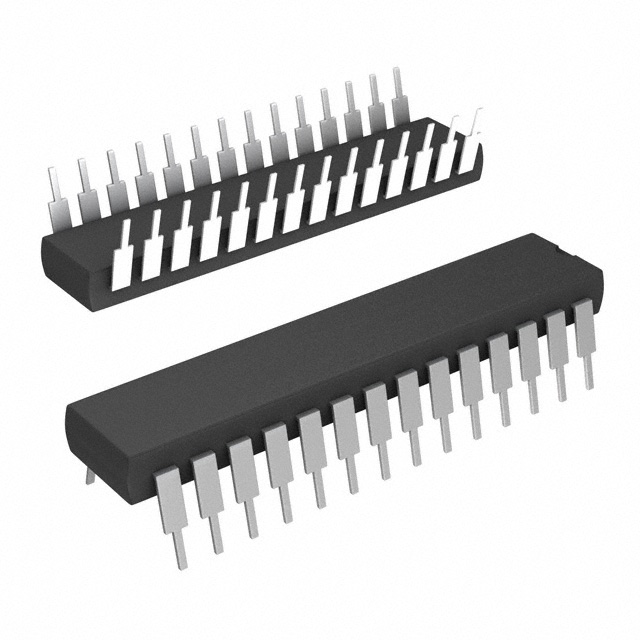
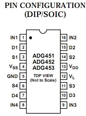
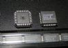
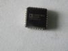
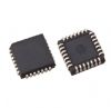
ADG453: Features: 44 V Supply Maximum Ratings615 V Analog Signal RangeContinuous Current 100 mAFast Switching Times tON 70 ns tOFF 60 nsTTL/CMOS CompatiblePin Compatible Upgrade for ADG411/ADG412/ADG413 and...
 ADG453 Data Sheet
floor Price/Ceiling Price
- Part Number:
- ADG453
- Supply Ability:
- 5000
Price Break
- Qty
- 1~5000
- Unit Price
- Negotiable
- Processing time
- 15 Days
SeekIC Buyer Protection PLUS - newly updated for 2013!
- Escrow Protection.
- Guaranteed refunds.
- Secure payments.
- Learn more >>
Month Sales
268 Transactions
Payment Methods
All payment methods are secure and covered by SeekIC Buyer Protection PLUS.
Notice: When you place an order, your payment is made to SeekIC and not to your seller. SeekIC only pays the seller after confirming you have received your order. We will also never share your payment details with your seller.