Mounting Type: Surface Mount
Operating Temperature: -40°C ~ 85°C
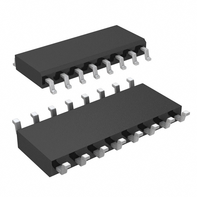
Package / Case: 16-SOIC (0.154", 3.90mm Width)
Series: -
Circuit: 2 x 4:1
Current - Supply: 100nA
Packaging: Tube
Function: Multiplexer
Voltage Supply Source: Dual Supply
Voltage - Supply, Single/Dual (±): ±15V
Supplier Device Package: 16-SOIC
Manufacturer: Analog Devices Inc
On-State Resistance: 300 Ohm
DescriptionThe ADG509FBRNZ is one member of the ADG509F series.The ADG509FBRNZ is CMOS analog multiplexer,the ADG509F comprising four differential channels.These multiplexers provide fault protection. Using a series n-channel, p-channel, n-channel MOSFET structure, both device and signal source protection is provided in the event of an overvoltage or power loss. The multiplexer can withstand continuous overvoltage inputs from 40 V to +55 V.During fault conditions, the multiplexer input (or output) appears as an open circuit and only a few nanoamperes of leakage current will flow.This protects not only the multiplexer and the circuitry driven by the multiplexer, but also protects the sensors or signal sources that drive the multiplexer.
Features of the ADG509FBRNZ are:(1)low power dissipation (3.3 mW max); (2)fault and overvoltage protection (40 V to +55 V); (3)all switches OFF with power supply OFF; (4)analog output of ON channel clamped within power supplies if an overvoltage occurs; (5)latch-up proof construction; (6)break before make construction; (7)TTL and CMOS compatible inputs.During fault conditions, the leakage current into and out of the ADG509F is limited to a few microamps.This protects the multiplexer and succeeding circuitry from over stresses as well as protecting the signal sources which drive the multiplexer. Also, the other channels of the multiplexer will be undisturbed by the overvoltage and will continue to operate normally.
The absolute maximum ratings of the ADG509FBRNZ can be summarized as:(1)Vdd to Vss:+44V;(2)storage temperature:-65 to 150;(3)peak current:40mA;(4)junction temperature:150;(5)Vdd to GND:-0.3 to +25V.Stresses above those listed under Absolute Maximum Ratings may cause permanent damage to the device.This is a stress rating only;functional operation of the device at these or any other conditions above those listed in the operational sections of this specification is not implied.Exposure to absolute maximum rating conditions for extended periods may affect device reliability.Only one absolute maximum rating may be applied at any one time.Finally, when the power supplies are off, the gate of each MOSFET will be at ground. A negative overvoltage switches on the first n-channel MOSFET but the bias produced by the overvoltage causes the p-channel MOSFET to remain turned off.With a positive overvoltage, the first MOSFET in the series will remain off since the gate to source voltage applied to this MOSFET is negative.
Parameters: | Technical/Catalog Information | ADG509FBRNZ |
| Vendor | Analog Devices Inc |
| Category | Integrated Circuits (ICs) |
| Type | Multiplexer |
| Voltage Supply Source | Dual Supply |
| Voltage - Supply, Single/Dual (±) | ±10.8 V ~ 16.5 V |
| Circuit | 2 x 4:1 |
| On-State Resistance | 300 Ohm |
| Mounting Type | Surface Mount |
| Package / Case | 16-SOIC (3.9mm Width) |
| Packaging | Tube |
| Current - Supply | 20A |
| Operating Temperature | -40°C ~ 85°C |
| Function | Multiplexer |
| Drawing Number | * |
| Lead Free Status | Lead Free |
| RoHS Status | RoHS Compliant |
| Other Names | ADG509FBRNZ
ADG509FBRNZ
|
 ADG509FBRNZ Data Sheet