Features: `±2 V to ±6 V Dual Supply
`2 V to 12 V Single Supply
`Automotive Temperature Range 40oC to +125
`<0.2 nA Leakage Currents
`52 On Resistance over Full Signal Range
`Rail-to-Rail Switching Operation
`16-Lead Chip Scale/TSSOP Package
`Typical Power Consumption <0.1 W
`TTL/CMOS Compatible Inputs
`Package Upgrades to 74HC4053 and MAX4053/MAX4583Application·Automotive Applications
·Automatic Test Equipment
·Data Acquisition Systems
·Battery Powered Systems
·Communication Systems
·Audio and Video Signal Routing
·Relay Replacement
·Sample-and-Hold Systems
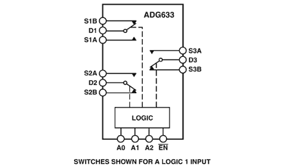
·Industrial Control SystemsPinout
 Specifications
| Switch Type |
SPDT |
| # Channels |
3 |
| Ron (Ohms) |
52Ohms |
| Id, Is (ON) |
5pA |
| Bandwidth |
580MHz |
| t ON |
70ns |
| t OFF |
25ns |
| Supply Voltage |
Dual (±5V),Single (+12V),Single (+2.7V to +5.5V),Single (+3.3V),Single (+3V),Single (+5V) |
(TA = 25, unless otherwise noted.)
VDD to VSS........................................................................ 13 V
VDD to GND...................................................... 0.3 V to +13 V
VSS to GND...................................................... +0.3 V to 6.5 V
Analog Inputs2.................................VSS 0.3 V to VDD + 0.3 V
Digital Inputs2.................................GND 0.3 V to VDD + 0.3 V
or 10 mA, whichever occurs fi rst
Peak Current, S or D......................................................... 40 mA
(Pulsed at 1 ms, 10% duty cycle max)
Continuous Current, S or D...............................................20 mA
Operating Temperature Range
Automotive (Y Version)..................................40 to +125
Industrial (B Version)....................................... 40 to +85
Storage Temperature Range..............................65 to +150
Junction Temperature.......................................................... 150
JA Thermal Impedance, 16-Lead TSSOP......................150.4/W
JA Thermal Impedance (4-Layer Board),
16-Lead LFCSP...............................................................70/W
Lead Temperature, Soldering
Vapor Phase (60 sec)........................................................215
Infrared (15 sec)...............................................................220
ESD....................................................................................... 4 kV
NOTES
1Stresses above those listed under Absolute Maximum Ratings may cause permanent damage to the device. This is a stress rating only; functional operation of the device at these or any other conditions above those listed in the operational sections of this specifi cation is not implied. Exposure to absolute maximum rating conditions for extended periods may affect device reliability. Only one absolute maximum rating may be applied at any one time.
2Overvoltages at AX, EN, S, or D will be clamped by internal diodes. Current should be limited to the maximum ratings given.
DescriptionThe ADG633 is a low voltage CMOS device comprising three independently selectable SPDT (single pole double throw) switches. They are fully specif ed for ±5 V, +5 V, and +3 V supplies. The ADG633 switches are turned on with a logic low (or high) on the appropriate control input. Each switch conducts equally well in both directions when ON and has an input signal range that extends to the supplies. AnEN input is used to enable or EN EN disable the device. When disabled, all channels are switched off.
These parts are designed on an enhanced process that pro- vides lower power dissipation yet gives high switching speeds. Low power consumption and an operating supply range of 2 V to 12 V make the ADG633 ideal for battery-powered portable instruments. All channels exhibit break-before-make switching
action, preventing momentary shorting when switching chan- nels. All digital inputs have 0.8 V to 2.4 V logic thresholds, ensuring TTL/CMOS logic compatibility when using single +5 V or dual ±5 V supplies.
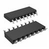
The ADG633 is available in small 16-lead TSSOP packages and 16-lead 4 mm 4 mm chip scale packages.

 ADG633 Data Sheet


