ADG707

Features: ` 1.8 V to 5.5 V Single Supply` ±3 V Dual Supply` 2.5 On Resistance` 0.5 On-Resistance Flatness` 100 pA Leakage Currents` 40 ns Switching Times` Single 16-to-1 Multiplexer ADG706` Differential 8-to-1 Multiplexer ADG707` 28-Lead TSSOP Package` Low-Power Consumption` TTL/CMOS-Compatible In...

product image

ADG707 Picture
SeekIC No. : 004275140 Detail

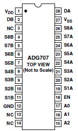
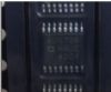
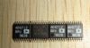
ADG707: Features: ` 1.8 V to 5.5 V Single Supply` ±3 V Dual Supply` 2.5 On Resistance` 0.5 On-Resistance Flatness` 100 pA Leakage Currents` 40 ns Switching Times` Single 16-to-1 Multiplexer ADG706` Differen...

floor Price/Ceiling Price

Part Number:
ADG707
Supply Ability:
5000

Price Break

  • Qty
  • 1~5000
  • Unit Price
  • Negotiable
  • Processing time
  • 15 Days
Total Cost: $ 0.00

SeekIC Buyer Protection PLUS - newly updated for 2013!

  • Escrow Protection.
  • Guaranteed refunds.
  • Secure payments.
  • Learn more >>

Month Sales

268 Transactions

Rating

evaluate  (4.8 stars)

Upload time: 2024/4/29

Payment Methods

All payment methods are secure and covered by SeekIC Buyer Protection PLUS.

Notice: When you place an order, your payment is made to SeekIC and not to your seller. SeekIC only pays the seller after confirming you have received your order. We will also never share your payment details with your seller.
Product Details

Description


Features:

` 1.8 V to 5.5 V Single Supply
` ±3 V Dual Supply
` 2.5 On Resistance
` 0.5 On-Resistance Flatness
` 100 pA Leakage Currents
` 40 ns Switching Times
` Single 16-to-1 Multiplexer ADG706
` Differential 8-to-1 Multiplexer ADG707
` 28-Lead TSSOP Package
` Low-Power Consumption
` TTL/CMOS-Compatible Inputs


Application

· Data Acquisition Systems
· Communication Systems
· Relay Replacement
· Audio and Video Switching
· Battery-Powered Systems


Pinout

  Connection Diagram


ADG707 Diagram


Specifications

VDD to VSS . . . . . . . . . . . . . . . . . . . . . . . . . . . . . . . . . . . 7 V
VDD to GND . . . . . . . . . . . . . . . . . . . . . . . . . . 0.3 V to +7 V
VSS to GND . . . . . . . . . . . . . . . . . . . . . . . . . +0.3 V to 3.5 V
Analog Inputs2 . . . . . . . . . . . . VSS 0.3 V to VDD + 0.3 V or
30 mA, Whichever Occurs First
Digital Inputs2 . . . . . . . . . . . . . . . . 0.3 V to VDD + 0.3 V or
30 mA, Whichever Occurs First
Peak Current, S or D . . . . . . . . . . . . . . . . . . . . . . . ..100 mA
(Pulsed at 1 ms, 10% Duty Cycle max)
Continuous Current, S or D . . . . . . . . . . . . . . . . . . . . 30 mA
Operating Temperature Range
Industrial (B Version) . . . . . . . . . . . . . . . . ..40°C to +85°C
Storage Temperature Range . . . . . . . . . . 65°C to +150°C
Junction Temperature . . . . . . . . . . . . . . . . . . . . . . . .. 150°C
TSSOP Package
JA Thermal Impedance . . . . . . . . . . . . . . . . . . . .. 97.9°C/W
JC Thermal Impedance . . . . . . . . . . . . . . . . . . . . . . 14°C/W
Lead Temperature, Soldering (10 seconds) . . . . . . . .. 300°C
IR Reflow, Peak Temperature . . . . . . . . . . . . . . . . . . . 220°C

NOTES
1Stresses above those listed under Absolute Maximum Ratings may cause permanent damage to the device. This is a stress rating only, functional operation of the device at these or any other conditions above those listed in the operational sections of this specification is not implied. Exposure to absolute maximum rating conditions for extended periods may affect device reliability. Only one absolute maximum rating may be applied at any one time.
2Overvoltages at IN, S or D will be clamped by internal diodes. Current should be limited to the maximum ratings given.


Sw/Mx Function x # (8:1) x 2
Interface Type Parallel
Available Packages SOP
Max Analog Signal Range Vss to Vdd
Ron (Ohms) 2.5Ohms
Ron Match (Ohms) 0.3Ohms
Cs (OFF) 13pF
Cs, Cd (ON) 100pF
Off Isolation (-dB) 80dB
Bandwidth 36MHz


Description

The ADG706 and ADG707 are low-voltage, CMOS analog multiplexers comprising 16 single channels and eight differential channels respectively. The ADG706 and ADG707  switches one of 16 inputs (S1S16) to a common output, D, as determined by the 4-bit binary address lines A0, A1, A2, and A3. The ADG707 switches one of eight differential inputs to a common differential output as determined by the 3-bit binary address lines A0, A1, and A2. An EN input on both devices is used to enable or disable the device. When disabled, all channels are switched OFF.

Low-power consumption and operating supply range of 1.8 V to 5.5 V make the ADG706 and ADG707 ideal for battery-powered, portable instruments. All channels exhibit break-before-make switching action preventing momentary shorting when switching channels. These devices are also designed to operate from a dual supply of ±3 V.

ADG706 and ADG707  multiplexers are designed on an enhanced submicron process that provides low-power dissipation yet gives highswitching speed, very low on resistance and leakage currents. On resistance is in the region of a few ohms and is closely matched between switches and very flat over the full signal range. These parts can operate equally well as either multiplexers or demultiplexers and have an input signal range which extends to the supplies.

The ADG706 and ADG707 are available in small 28-lead TSSOP packages.


Customers Who Bought This Item Also Bought

Margin,quality,low-cost products with low minimum orders. Secure your online payments with SeekIC Buyer Protection.
Fans, Thermal Management
Motors, Solenoids, Driver Boards/Modules
Cable Assemblies
Isolators
Inductors, Coils, Chokes
View more