Features: Broadband RF, IF, and LO ports Conversion loss: 6 dB Noise figure: 6 dB High input IP3: 26 dBm High input P1dB: 17 dBm Low LO drive level Single-ended design: no need for baluns Single-supply operation: 3 V @ 10 mA Miniature 8-lead 3 mm x 2 mm LFCSP package RoHS compliantApplicationCell...
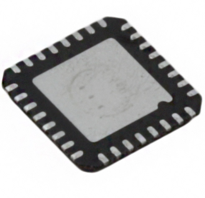
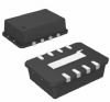
ADL5350: Features: Broadband RF, IF, and LO ports Conversion loss: 6 dB Noise figure: 6 dB High input IP3: 26 dBm High input P1dB: 17 dBm Low LO drive level Single-ended design: no need for baluns Single-su...
SeekIC Buyer Protection PLUS - newly updated for 2013!
268 Transactions
All payment methods are secure and covered by SeekIC Buyer Protection PLUS.


| Parameter | Rating |
| Supply Voltage, VS RF Input Level LO Input Level Internal Power Dissipation JA Maximum Junction Temperature Operating Temperature Range Storage Temperature Range |
6.0 V 20 dBm 20 dBm 324 mW 154.3 °C/W 135°C −40°C to +85°C −65°C to +150°C |
| RF Frequency (MHZ) | LF to 4000 |
| IF Frequency (MHz) | LF to 4000 |
| LO Frequency (MHz) | LF to 4000 |
| LO Drive (dBm) | +4 |
| IP3 (dBm) | 25 |
| P1dB (dBm) | 19 |
| Voltage Supply (V) | +5V |
| Supply Current | 19mA |
| Package | 8-Lead LFCSP |
The ADL5350 is a high linearity, up-and-down converting mixer capable of operating over a broad input frequency range. It is well suited for demanding cellular base-station mixer designs that require high sensitivity and efficient blocker immunity. Based on a GaAs pHEMT single-ended mixer architecture, the ADL5350 provides excellent input linearity and low noise figure without the need for a high power level, local oscillator (LO) drive.
In 850 MHz/900 MHz receive applications, the ADL5350 provides a typical conversion loss of only 6 dB. The integrated LO amplifier allows a low LO drive level, typically only 4 dBm for most applications. The input IP3 is typically greater than 25 dBm, with an input compression point of 17 dBm. The high input linearity of the ADL5350 makes the device an excellent mixer for communications systems that require high blocker immunity, such as GSM 850/900 and 800 MHz CDMA2000. At 2 GHz, a slightly greater supply current is required to obtain similar performance.
For low frequency applications, the ADL5350 provides access to the gate contact of the output-mixing device. This allows an external LO coupling capacitor to be applied between the VPOS pin and GC pin, helping to improve the LO drive to the switching device. Using a single 100 pF capacitor allows high performance at the lower LO frequencies. The single-ended broadband RF/IF port allows the device to be customized for a desired band of operation using simple external filter networks. The LO to RF isolation is based on the LO rejection of the RF port filter network. Greater isolation may be achieved using higher order filter networks as described in the Applications section of this data sheet.
The ADL5350 is fabricated on a GaAs pHEMT high performance IC process. The ADL5350 is available in a 3 mm × 2 mm 8-lead LFCSP package. It operates over a −40°C to +85°C temperature range. An evaluation board is also available.