Features: 3 Output Voltages (+5.1 V, +15.3 V, 10.2 V) from One 3 V Input SupplyPower Effciency Optimized for Use with TFT in Mobile PhonesLow Quiescent CurrentLow Shutdown Current (<1A)Fast Transient ResponseShutdown FunctionPower Saving during Blanking PeriodOption to Use External LDOApplicati...
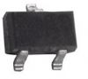
ADM8830: Features: 3 Output Voltages (+5.1 V, +15.3 V, 10.2 V) from One 3 V Input SupplyPower Effciency Optimized for Use with TFT in Mobile PhonesLow Quiescent CurrentLow Shutdown Current (<1A)Fast Trans...
SeekIC Buyer Protection PLUS - newly updated for 2013!
268 Transactions
All payment methods are secure and covered by SeekIC Buyer Protection PLUS.
(TA = 25°C, unless otherwise noted.)
Supply Voltage . . . . . . . . . . . . . . . . . . . . . . .0.3 V to +4.0 V
Input Voltage to Digital Inputs . . . . . . . . . . . 0.3 V to +4.0 V
Output Short Circuit Duration to GND . . . . . . . . . . . . . . .10 sec
Output Voltage
+5.1 V Output . . . . . . . . . . . . . . . . . . . . . . . . 0.3 V to +6 V
10.2 V Output . . . . . . . . . . . . . . . . . . . . . 12 V to +0.3 V
+15.3 V Output . . . . . . . . . . . . . . . . . . . . . . 0.3 V to +17 V
Operating Temperature Range . . . . . . . . . . 40°C to +85°C
Power Dissipation . . . . . . . . . . . . . . . . . . . . . . . . . . . . ...3.55 W
(Derate 33 mW/°C above 25°C)
Storage Temperature Range . . . . . . . . . . . 65°C to +150°C
ESD . . . . . . . . . . . . . . . . . . . . . . . . . . . . . . . . . . . . . . . . ..Class I
The ADM8830 is a charge pump regulator used for color thin flm transistor (TFT) liquid crystal displays (LCDs). Using charge pump technology, ADM8830 can be used to generate three output voltages (+5.1 V ± 2%, +15.3 V, 10.2 V) from a single 3 V input supply. These outputs are then used to provide supplies for the LCD controller (5.1 V) and the gate drives for the transistors in the panel (+15.3 V and 10.2 V). Only a fex external capacitors are needed for the charge pumps. An effcient low dropout voltage regulator also ensures that the power effciency is high and provides a low ripple 5.1 V output. This LDO can be shut down and an external LDO used to regulate the 5 V doubler output and drive the input to the charge pump section, which generates the +15.3 V and 10.2 V outputs if so required by the user.
The ADM8830 has an internal 100 kHz oscillator for use in scanning mode, but the part must be clocked by an external clock source in blanking (low current) mode. The internal oscillator is used to clock the charge pumps during scanning mode where the current is highest. During blanking periods, the ADM8830 switches to use an external, lower freque-ncy clock. This allows the user to vary the frequency and maximize power effciency during blanking periods. The to-lerances on the output voltages are seamlessly maintained when switching from scanning mode to blanking mode or vice versa.
The ADM8830 has a number of power saving features, including low power shutdown and reduced quiescent current consumption during the blanking periods mentioned above. The 5.1 V output consumes the most power, so power effciency is also maximized on this output with an oscillator enabling scheme (Green Idle™). This effectively senses the load current that is fowing and turns on the charge pump only when charge needs to be delivered to the 5 V pump doubler output.
The ADM8830 is fabricated using CMOS technology for minimal power consumption. The part is packaged in 20-lead LFCSP and TSSOP packages.