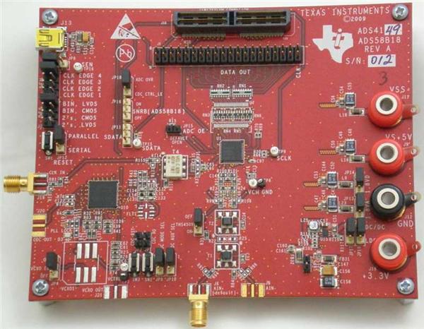
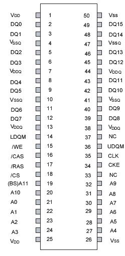
ADS4616A4A: Features: •Single 3.3V +/- 0.3V power supply•MRS Cycle with address key programs-CAS Latency (2 & 3)-Burst Length (1,2,4,8, & full page)-Burst Type (sequential & Interleave)&...
floor Price/Ceiling Price
- Part Number:
- ADS4616A4A
- Supply Ability:
- 5000
Price Break
- Qty
- 1~5000
- Unit Price
- Negotiable
- Processing time
- 15 Days
SeekIC Buyer Protection PLUS - newly updated for 2013!
- Escrow Protection.
- Guaranteed refunds.
- Secure payments.
- Learn more >>
Month Sales
268 Transactions
Payment Methods
All payment methods are secure and covered by SeekIC Buyer Protection PLUS.

 ADS4616A4A Data Sheet


