Features: · Maximum Sample Rate: 40MSPS· 10-Bit Resolution· No Missing Codes· Power Dissipation: 768mW· CMOS Technology· Simultaneous Sample-and-Hold· 60.5dB SNR at 10MHz IF· Serialized LVDS Outputs Meet or Exceed Requirements of ANSI TIA/EIA-644-A Standard· Internal and External References· 3.3V ...
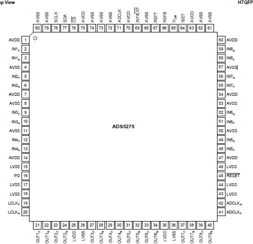
ADS5275: Features: · Maximum Sample Rate: 40MSPS· 10-Bit Resolution· No Missing Codes· Power Dissipation: 768mW· CMOS Technology· Simultaneous Sample-and-Hold· 60.5dB SNR at 10MHz IF· Serialized LVDS Outputs...
SeekIC Buyer Protection PLUS - newly updated for 2013!
268 Transactions
All payment methods are secure and covered by SeekIC Buyer Protection PLUS.

| Supply Voltage Range, AVDD | -0.3V to +3.8V |
| Supply Voltage Range, LVDD | -0.3V to +3.8V |
| Voltage Between AVSS and LVSS | -0.3V to +0.3V |
| Voltage Between AVDD and LVDD | -0.3V to +0.3V |
| Voltage Applied to External REF Pins | -0.3V to +2.4V |
| All LVDS Data and Clock Outputs | -0.3V to +2.4V |
| Analog Input Pins | 0.3V to +2.7V |
| Peak Total Input Current (all inputs) | -30mA |
| Operating Free-Air Temperature Range, TA | -40 to +85 |
| Lead Temperature, 1.6mm (1/16" from case for 10s) | 220 |
(1) Stresses above these ratings may cause permanent damage. Exposure to absolute maximum conditions for extended periods may degrade device reliability. These are stress ratings only, and functional operation of the device at these or any other conditions beyond those specified is not supported.
The ADS5275 is a high-performance, 40MSPS, 8-channel, parallel analog-to-digital converter (ADC). Internal references are provided, simplifying system design requirements. Low power consumption allows for the highest of system integration densities. Serial LVDS (low-voltage differential signaling) outputs reduce the number of interface lines and package size.
In LVDS, an integrated phase lock loop multiplies the incoming ADC sampling clock by a factor of 6. This high-frequency LVDS clock is used in the data serialization and transmission process and is converted to an LVDS signal for transmission in parallel with the data. Providing this additional LVDS clock allows for easy delay matching. The word output of each internal ADC is serialized and transmitted either MSB or LSB first. The bit following the rising edge of the ADC clock output is the first bit of the word.The ADS5275 provides internal references, or can 40MSPS optionally be driven with external references. Best performance can be achieved through the internal.The ADS5275 provides internal references, or can 40MSPS optionally be driven with external references. Best performance can be achieved through the internal.